Method for assembling a digitizer sensor

a technology of digitizer sensor and assembly method, which is applied in the field of assembly of digitizer sensor, can solve the problems that traditional methods of establishing electrical and mechanical contact between two substrates such as soldering or using anisotropic conductive paste (acp) or film (acf) cannot be used

Inactive Publication Date: 2009-12-31
N TRIG
View PDF8 Cites 32 Cited by
  • Summary
  • Abstract
  • Description
  • Claims
  • Application Information

AI Technical Summary

Benefits of technology

[0010]According to an aspect of some embodiments of the present invention there is provided a method for mounting a PCB or like substrate on a digitizer sensor so as to establish electrical connection between conductive lines patterned on the digitizer sensor and matching contact points patterned on the PCB while avoiding shorti

Problems solved by technology

Since substrates such as PET foil and glass are typically heat sensitive, traditional methods for establishing electrical and mec

Method used


Image

  • Method for assembling a digitizer sensor
  • Method for assembling a digitizer sensor
  • Method for assembling a digitizer sensor

Examples


Embodiment Construction

[0064]The present invention, in some embodiments thereof, relates to assembly of digitizer sensors and, more particularly, but not exclusively, to methods for establishing electrical connection between conductive material of the digitizer sensor and electrical components associated with the sensor.

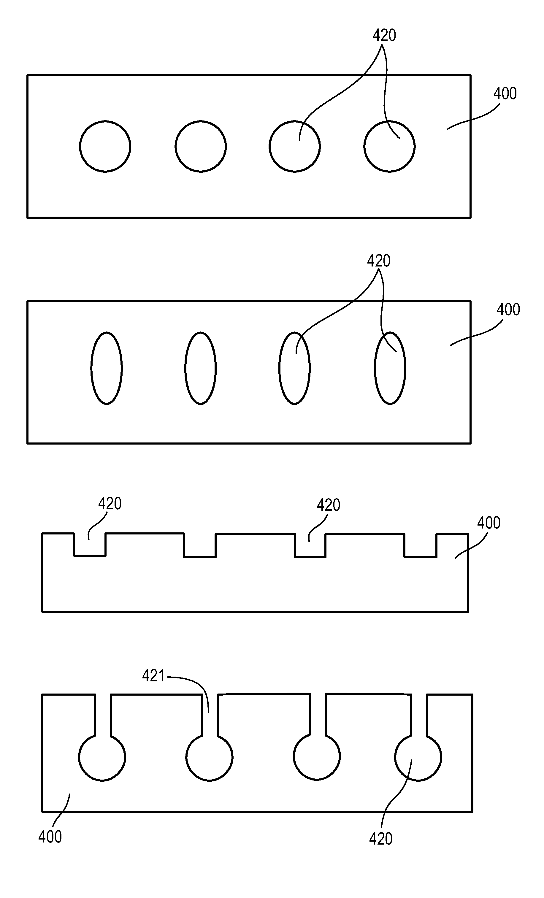
[0065]An aspect of some embodiments of the present inventions provides for using non-conductive Double Sided Adhesive (DSA) formed with holes, gaps or openings to bind a PCB or like substrate to a digitizer sensor. The holes, gaps or opening are formed to correspond to discrete areas where electrical contact is required between the PCB and the digitizer sensor. According to some embodiments of the present invention, the holes, gaps or opening formed provide a volume within which conductive material can be deposited so that electrical contact can be established between the PCB and sensor in the discrete areas where electrical contact is required. Additionally, the non-conductive material de...


PUM

PropertyMeasurementUnit
Sizeaaaaaaaaaa
Electrical conductoraaaaaaaaaa
Transparencyaaaaaaaaaa

Abstract

A digitizer assembly includes a transparent sensor patterned with conductive elements within at least one layer, a PCB or the like patterned with conductive elements positioned along at least one edge of the transparent sensor, wherein the conductive elements at least partially match the conductive elements on the transparent sensor, and a double sided adhesive positioned between the transparent sensor and the PCB operative to mount the PCB on to the transparent sensor.

Description

RELATED APPLICATION[0001]The present application claims the benefit under section 35 U.S.C. §119(e) of U.S. Provisional Patent Application No. 61 / 129,308 filed on Jun. 18, 2008, which is incorporated herein by reference in its entirety.FIELD OF THE INVENTION[0002]The present invention, in some embodiments thereof, relates to assembly of digitizer sensors and, more particularly, but not exclusively, to methods for establishing electrical connection between conductive elements on the sensor and electrical components associated with the sensor.BACKGROUND OF THE INVENTION[0003]Digitizing systems that allow a user to operate a computing device with a stylus and / or finger are known. Typically, a digitizer is integrated with a display screen, e.g. over-laid on the display screen, to correlate user input, e.g. stylus interaction and / or finger touch on the screen with the virtual information portrayed on display screen.[0004]Typically, the digitizer systems include a digitizer sensor formed ...

Claims


Application Information

Patent Timeline
IPC IPC(8): G06F3/041B32B37/02
CPCY10T156/10G06F3/041G06F3/04164
Inventor YAAKOBY, MERAVTEOMIM, DORONNACHSHON, DOVBRECHER, DOVKAIMONOVICH, ALEX
Owner N TRIG
Why Eureka
Try Eureka