Bga package

a technology of ball grid array and package, which is applied in the direction of printed circuit, sustainable manufacturing/processing, final product manufacturing, etc., can solve the problems of affecting the quality of bga packages, so as to reduce failures and breakdowns.

Inactive Publication Date: 2010-01-14
NEC CORP
View PDF3 Cites 5 Cited by
  • Summary
  • Abstract
  • Description
  • Claims
  • Application Information

AI Technical Summary

Benefits of technology

[0009]This invention has been made in order to solve problems associated with the related arts described above, and it is an object of this invention to provide a BGA package capable of reducing failures and breakdowns caused by peeling of terminal pads.

Problems solved by technology

Some devices having a multiplicity of terminals like a conventional small-sized BGA suffer breakdowns due to peeling of square terminal pads possibly caused by the devices being dropped or subjected to a shock.
Even though a device apparently does not seem damaged significantly, it may be severely damaged in the inside thereof.
It is very difficult in practice to determine for an LSI in a BGA package whether and how it is damaged.

Method used


Image

  • Bga package
  • Bga package
  • Bga package

Examples


Embodiment Construction

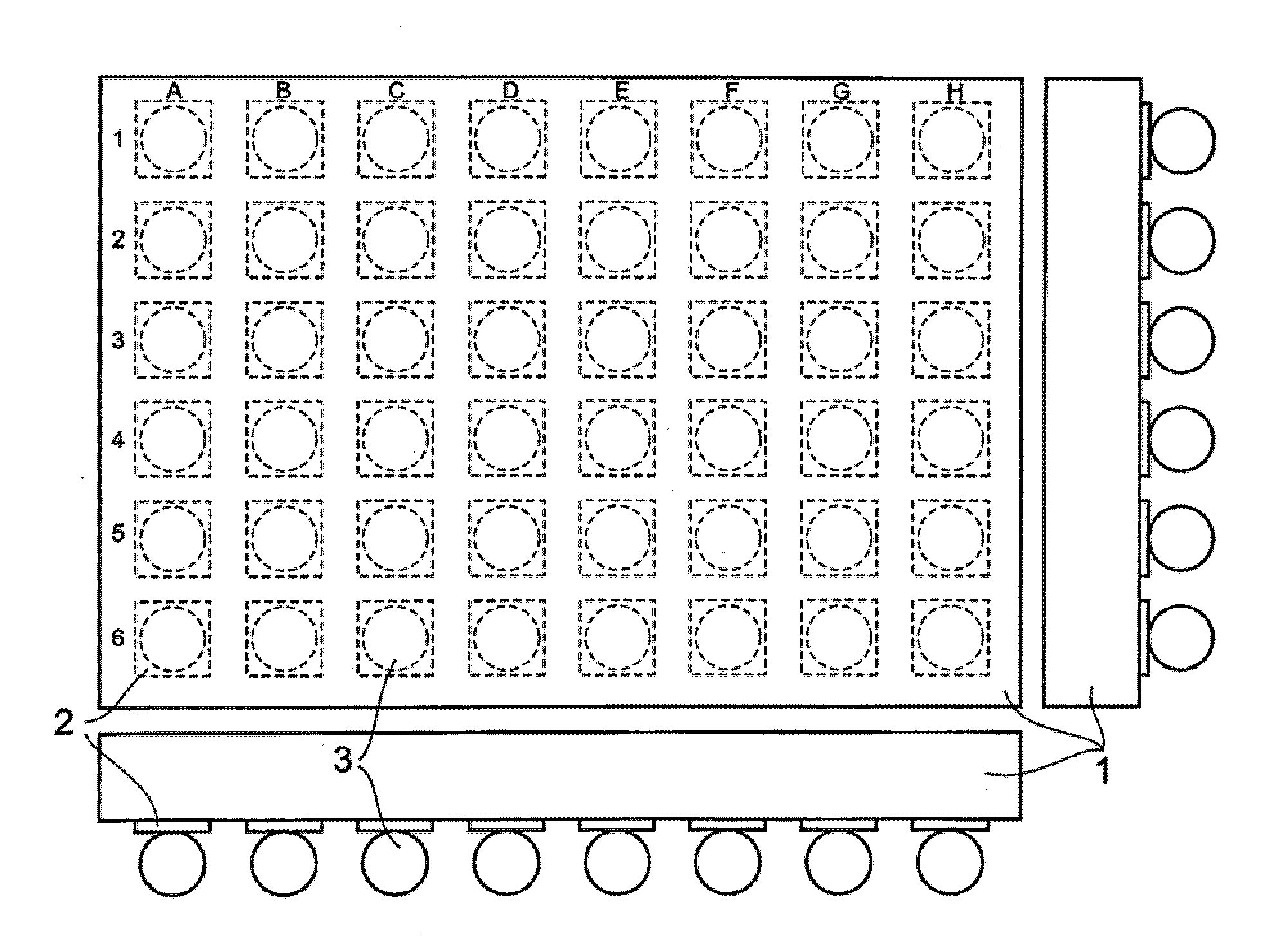
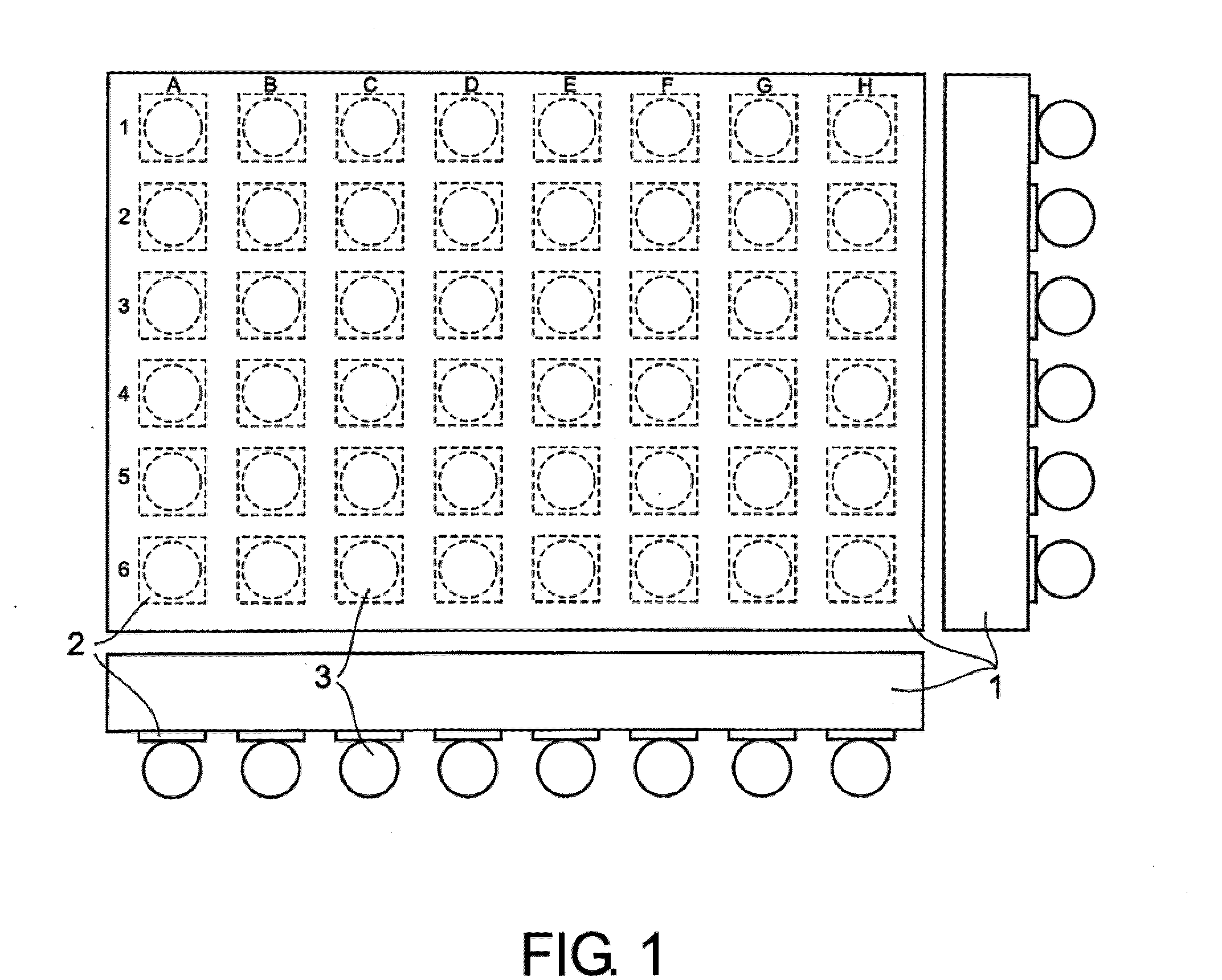
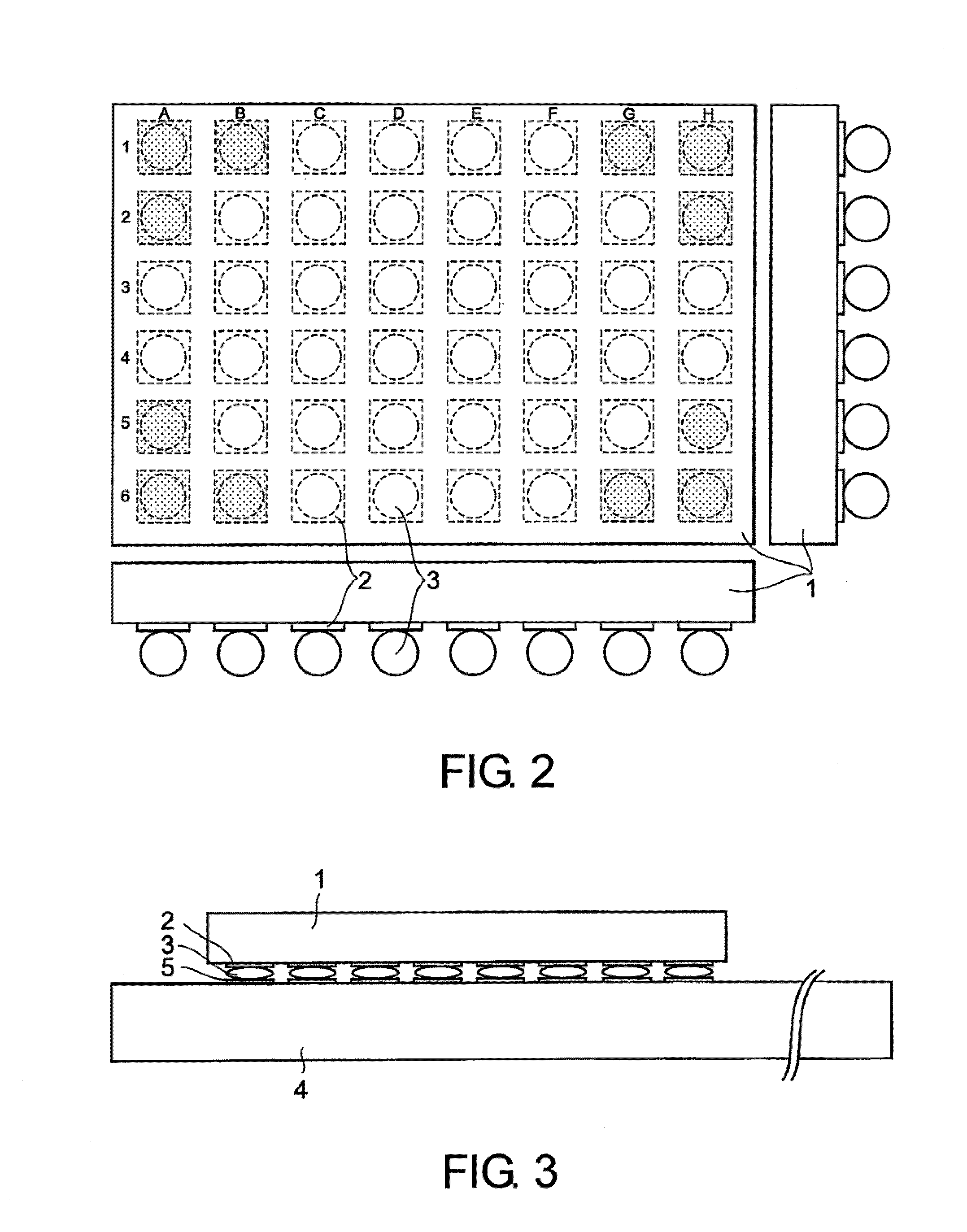
[0016]First, a known type of BGA package will be described with reference to FIG. 1 to FIG. 3.

[0017]As shown in FIGS. 1 to 3, this known BGA package has an LSI package 1, a plurality of terminal pads 2 arranged in a grid pattern on the rear surface of the LSI package 1, and solder balls 3 for soldering the LSI package 1 to terminal pads 5 on a printed wiring board 4 via the terminal pads 2.

[0018]Among the terminal pads 2 of the known BGA package, those terminal pads at the four corners (three pads at each of the corners) are weak and prone to peeling. FIG. 2 shows the terminal pads at the four corners which are possibly broken. Specifically, three terminal pads 2 arranged at the positions 1-A, 1-B, 2-A at the upper left corner of the grid-like layout, three terminal pads 2 at the positions 5-A, 6-A, 6-B at the lower left corner, three terminal pads 2 at the positions 1-G, 1-H, 2-H at the upper right corner, and three terminal pads 2 at the positions 5-H, 6-G, 6-H at the lower right ...


PUM


Abstract

A BGA package has an LSI package, a plurality of terminal pads arranged in a grid pattern on the rear surface of the LSI package, and solder balls for soldering the LSI package to a printed wiring board via the terminal pads. A plurality of the terminals pads located at each of the four corners of the outermost periphery of the LSI package form a group of first terminal pads, and each group of terminal pads is formed integrally as a reinforcing pad having a greater size than that of the other terminal pads.

Description

[0001]This application is based upon and claims the benefit of priority from Japanese patent application No. 2008-179416, filed on Jul. 9, 2008, the disclosure of which is incorporated herein in its entirety by reference.FIELD OF THE INVENTION[0002]This invention relates to a BGA (ball grid array) package and, in particular, to a BGA package for preventing peeling of terminal pads.DESCRIPTION OF THE RELATED ART[0003]Some devices having a multiplicity of terminals like a conventional small-sized BGA suffer breakdowns due to peeling of square terminal pads possibly caused by the devices being dropped or subjected to a shock.[0004]Even though a device apparently does not seem damaged significantly, it may be severely damaged in the inside thereof. It is very difficult in practice to determine for an LSI in a BGA package whether and how it is damaged.[0005]Techniques relating to this are described for example in Japanese Laid-Open Patent Publication No. 2001-244585 (Patent Document 1), ...

Claims


Application Information

Patent Timeline
Patent Type & Authority Applications(United States)
IPC IPC(8): H01L23/498
CPCH01L23/3114H01L23/49816H01L23/562H05K3/3436H05K2201/094H01L2924/0002H05K2203/0465H01L2924/00Y02P70/50
Inventor SANO, AKIHIRO
Owner NEC CORP
Why Eureka
Try Eureka