Synthesis and Use of Precursors for ALD of Tellurium and Selenium Thin Films

a technology of tellurium and selenium, which is applied in the direction of organic compounds without c-metal linkages, organic chemistry, coatings, etc., can solve the problems of inability to form complex 3-d cell structures, limited atomic layer deposition processes for te and se-containing thin films, and lack of precursors

Active Publication Date: 2010-01-14
ASM INTERNATIONAL
View PDF20 Cites 35 Cited by
  • Summary
  • Abstract
  • Description
  • Claims
  • Application Information

AI Technical Summary

Benefits of technology

[0010]The methods disclosed herein provide reliable atomic layer deposition (ALD) methods for forming thin films comprising tellurium and for making precursors that can be used in such methods.

Problems solved by technology

Sputtering may be capable of forming simple pore and trench structures, however, future PCM applications will require more complicated 3-D cell structures that cannot be formed using sputtering techniques.
Atomic layer deposition processes for depositing Te and Se-containing thin films have been limited, in part, by a lack of appropriate precursors.

Method used


Image

  • Synthesis and Use of Precursors for ALD of Tellurium and Selenium Thin Films
  • Synthesis and Use of Precursors for ALD of Tellurium and Selenium Thin Films
  • Synthesis and Use of Precursors for ALD of Tellurium and Selenium Thin Films

Examples


example 1

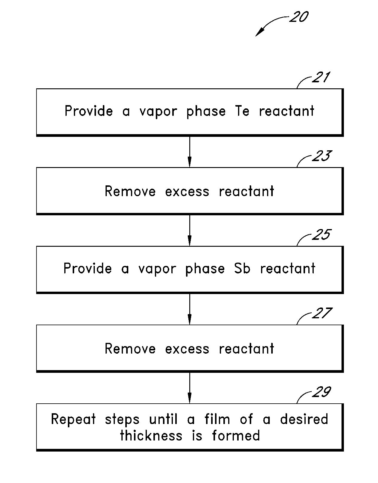
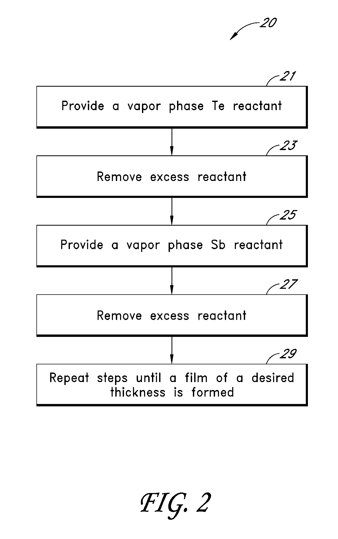
[0104]Sb—Te thin films were formed using alternating and sequential pulses of SbCl3 and Te(SiMe2tBu)2. Pulse and purge lengths were 1 and 2 seconds for SbCl3 and 1 and 4 seconds for Te(SiMe2tBu)2. Sb—Te thin films were grown at approximately 100° C. on a silicon surface, soda lime glass, and rhodium. The Sb—Te thin films were deposited to a thickness between about 9 nm and about 12 nm.

[0105]The morphology of each film was compared using FESEM (field emission scanning electron microscope) images. In the FESEM images there were visible isolated islands on the film formed on the silicon substrate. However, the films grown on soda lime glass and rhodium were continuous.

example 2

[0106]Sb—Te films were deposited on silicon and on tungsten at approximately 150° C. using Te(SiEt3)2 as the Te source and SbCl3 as the Sb source. The SbCl3 pulse length was about 1 second and the purge length was about 2 seconds. The Te(SiEt3)2 pulse length was varied between about 0.2 seconds and 2.0 seconds while the purge length was about 2 seconds. The growth rate and composition were measured for the thin films formed with varying Te precursor pulse lengths. The results are illustrated in FIGS. 3-5, which also show error bars for each point estimating the uncertainty associated with the EDX measurement technique. As can be seen in FIG. 3, the growth rate per cycle ranged from about 0.019 to 0.025 Å / cycle on silicon with native oxide and from about 0.023 to 0.073 Å / cycle on tungsten depending on Te precursor pulse length. The exact composition of the films also varied with the pulse length of the Te precursor on silicon with native oxide (FIG. 4) and tungsten (FIG. 5).

[0107]FIG...

example 3

[0113]Sb—Te films were deposited on a substrate using Te(SiEt3)2 as the Te source and SbCl3 as the Sb source at varying temperatures and varying precursor pulse lengths. FIG. 19 is a graph of the composition of a Sb—Te thin film deposited on a tungsten substrate at varying growth temperatures. The Sb—Te thin films were deposited using 1 second pulses of Te(SiEt3)2 and SbCl3 reactants along with a 2 second purge between each reactant pulse. The deposited Sb—Te film was close to the stoichiometric ratio of Sb2Te3 for temperatures of about 100° C. and below. Additionally, no chlorine impurities were detected by EDX analysis. For higher temperatures, above about 120° C., the Sb—Te films contained slightly more antimony than the stoichiometric ratio of Sb2Te3.

[0114]FIG. 20 is a graph of the average growth rate per cycle of Sb—Te versus the growth temperature for Sb—Te deposited on a tungsten substrate and a silicon substrate. The Sb—Te thin films were deposited using 1 second pulses of T...


PUM

PropertyMeasurementUnit
deposition temperatureaaaaaaaaaa
temperatureaaaaaaaaaa

Abstract

Atomic layer deposition (ALD) processes for forming Te-containing thin films, such as Sb—Te, Ge—Te, Ge—Sb—Te, Bi—Te, and Zn—Te thin films are provided. ALD processes are also provided for forming Se-containing thin films, such as Sb—Se, Ge—Se, Ge—Sb—Se, Bi—Se, and Zn—Se thin films are also provided. Te and Se precursors of the formula (Te,Se)(SiR1R2R3)2 are preferably used, wherein R1, R2, and R3 are alkyl groups. Methods are also provided for synthesizing these Te and Se precursors. Methods are also provided for using the Te and Se thin films in phase change memory devices.

Description

REFERENCE TO RELATED APPLICATIONS[0001]The present application claims priority under 35 U.S.C. § 119(e) to U.S. Provisional Application No. 61 / 048,077 filed Apr. 25, 2008; Ser. No. 61 / 112,128 filed Nov. 6, 2008; and Ser. No. 61 / 117,896 filed Nov. 25, 2008; entitled SYNTHESIS AND USE OF PRECURSORS FOR ALD OF TELLURIUM AND SELENIUM THIN FILMS, which are all hereby incorporated by reference in their entirety.PARTIES OF JOINT RESEARCH AGREEMENT[0002]The invention claimed herein was made by, or on behalf of, and / or in connection with a joint research agreement between the University of Helsinki and ASM Microchemistry signed on Nov. 14, 2003. The agreement was in effect on and before the date the claimed invention was made, and the claimed invention was made as a result of activities undertaken within the scope of the agreement.BACKGROUND OF THE INVENTION[0003]1. Field of the Invention[0004]The present application relates generally to methods and compounds for forming thin films comprisin...

Claims


Application Information

Patent Timeline
Patent Type & Authority Applications(United States)
IPC IPC(8): C23C16/455
CPCC23C16/306C23C16/45553H01L21/0256H01L21/02562H01L45/1616H01L45/06H01L45/1233H01L45/143H01L45/144H01L21/0262Y02P20/582H10N70/231H10N70/8825H10N70/826H10N70/8828H10N70/023C07F11/005
Inventor PORE, VILJAMIHATANPAA, TIMORITALA, MIKKOLESKELA, MARKKU
Owner ASM INTERNATIONAL
Why Eureka
Try Eureka