
Textile for connection of electronic devices

Inactive Publication Date: 2010-01-21
KONINKLIJKE PHILIPS ELECTRONICS NV
View PDF5 Cites 14 Cited by
  • Summary
  • Abstract
  • Description
  • Claims
  • Application Information

AI Technical Summary

Benefits of technology

[0006]In view of the above-mentioned and other drawbacks of the prior art, a general object of the present invention is to provide an improved textile for connection of electronic devices.
[0009]The textile according to the present invention provides a large number of connection paths to each pair of connection points for connection of an electronic device. Hereby, an electronic textile formed from the textile according to the present invention can be make very robust to cuts in the textile. In other words, even if many of the connection paths leading to a certain electronic device are broken, there is a high probability that some connection paths will remain so that the electronic device will be able to function as if nothing had happened. This means that the electronic textile, through the use of a textile according to the present invention, can be cut to measure without influencing the operation of the electronic devices in the electronic textile. With proper positioning of a power supply, or redundancy of power supplies, this is even the case when the electronic devices in the electronic textile are powered and operating.
[0016]In this way, the intermediate layer(s) of the multilayer weave are involved to a greater degree in the weaving, which enables the formation of a stronger weave having improved integrity. In cases when loops are formed by the first set of conductive weft yarns, these loops may, of course, analogously be formed around a larger number of non-conductive warp yarns in the intermediate layer than in the lower layer.

Problems solved by technology

This is a disadvantage of this type of electronic textiles, since textiles as a rule need to be cut into suitable shapes and measures in order to allow manufacturing of domestic textiles or clothes.

Method used


Image

  • Textile for connection of electronic devices
  • Textile for connection of electronic devices
  • Textile for connection of electronic devices

Examples


first embodiment

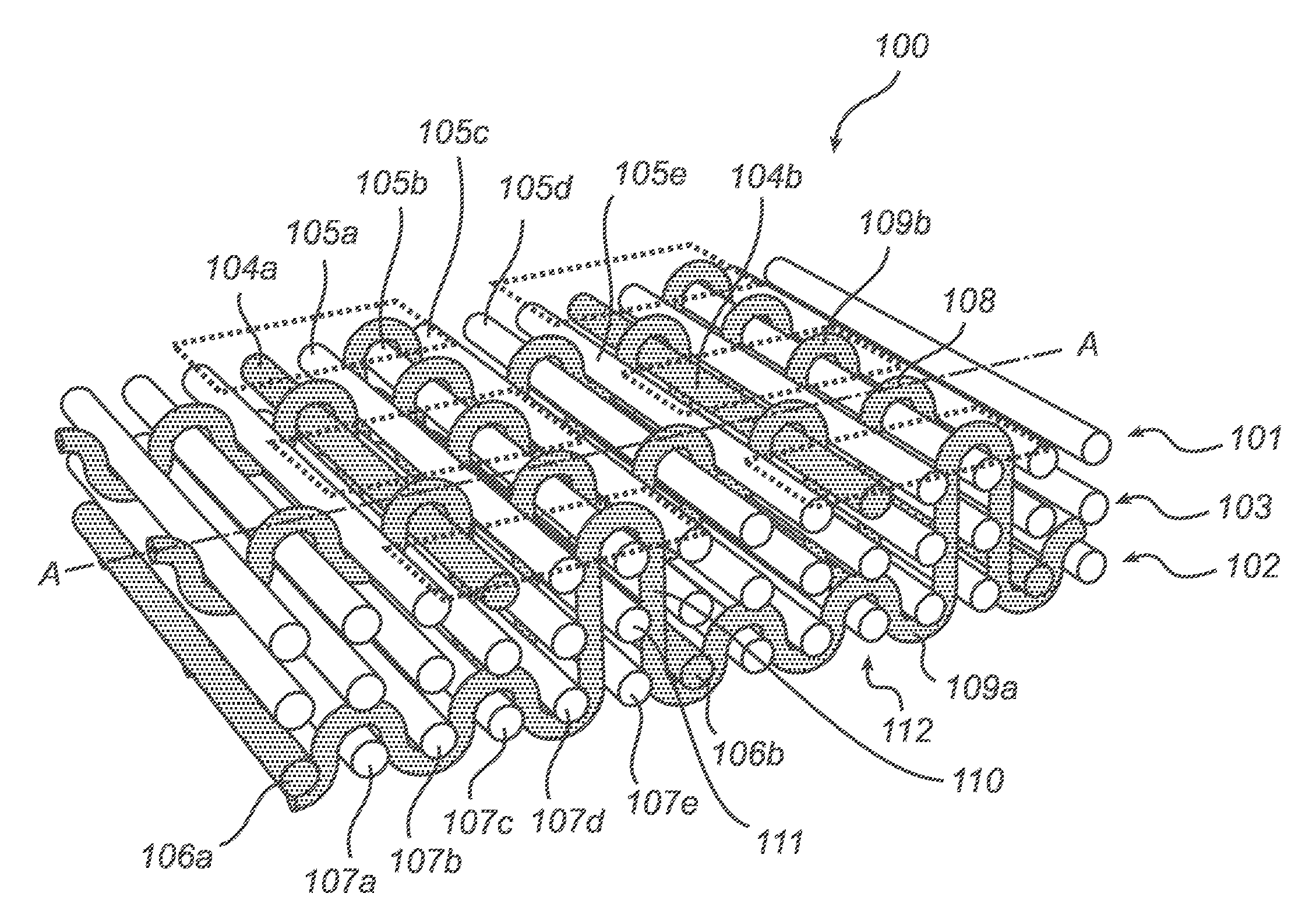
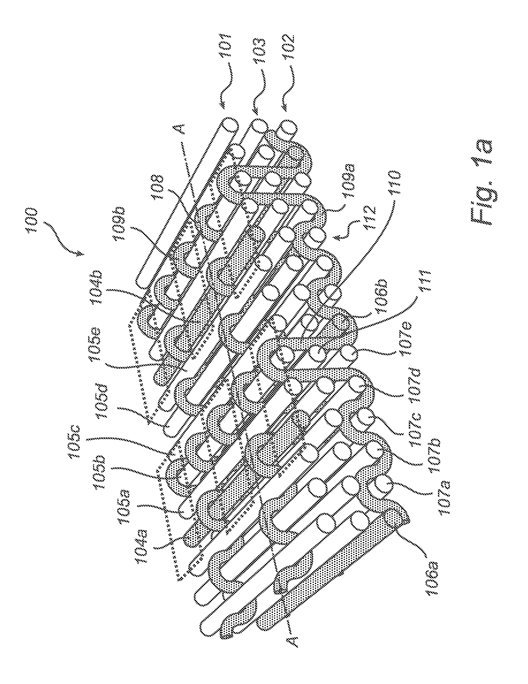
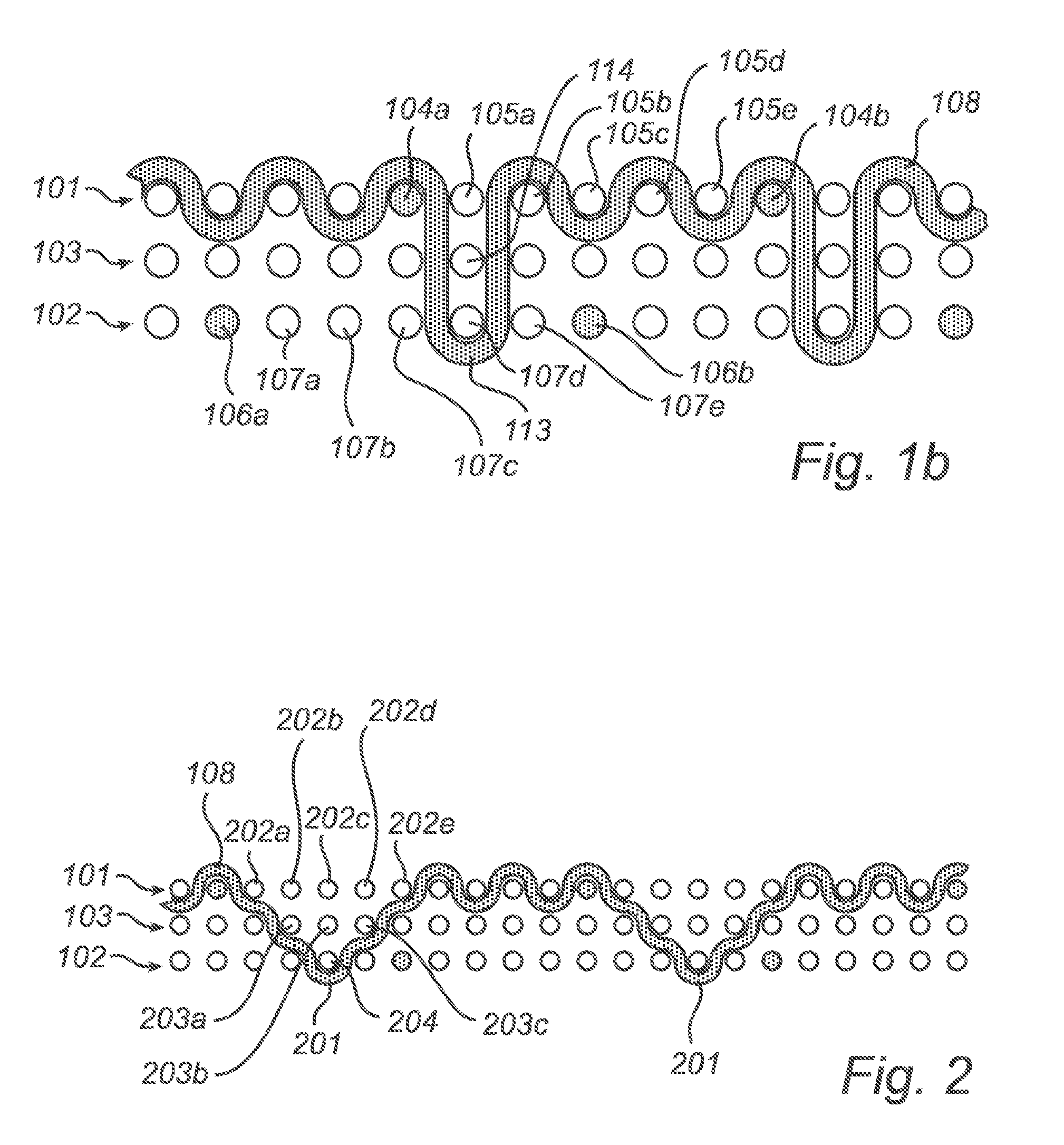
[0041]In FIG. 1a, a three-layer woven textile 100 according to the present invention is schematically shown having an upper 101 and a lower 102 warp layer which are separated by an intermediate warp layer 103. The upper warp layer 101 comprises an array of conductive warp yarns 104a-b separated by non-conductive warp yarns 105a-e, and the lower warp layer 102, in the presently illustrated example, has an identical, but translated, configuration of conductive 106a-b and non-conductive 107a-e warp yarns. The intermediate warp layer 103 here consists of all non-conductive warp yarns. However, this is not necessarily the case.

[0042]In the weft direction, one conductive weft yarn 108 from a first set of conductive weft yarns and two conductive weft yarns 109a-b from a second set of conductive weft yarns can be seen in FIG. 1a. Non-conductive weft yarns may be present between the conductive weft yarns shown in FIG. 1a, but have here been omitted for the sake of clarity.

[0043]Referring aga...

second embodiment

[0046]In FIG. 2, schematically illustrating the textile according to the present invention, loops 201 are shown, which are formed by conductive weft yarns 108 of the first set of conductive weft yarns, around non-conductive yarns 202a-e in the upper warp layer 101, non-conductive yarns 203a-c in the intermediate warp layer 103 and the non-conductive yarn 204 in the lower warp layer 102. According to this embodiment, the conductive weft yarns 108 interact to a greater degree with the warp yarns of the intermediate warp layer 103, leading to a better anchoring of the conductive weft yarns 108. FIG. 3 is a schematic view illustrating the robustness of an electronic textile utilizing a textile according to an embodiment of the present invention.

[0047]In FIG. 3, a conductor pattern of a portion of an electronic textile 300 is schematically shown, where the upper layer conductive grid 301 is indicated by the solid grid lines in rows 302a-f and columns 303a-e, and the lower layer conductiv...

third embodiment

[0051]With reference to FIGS. 4a-d, a textile 400 according to the present invention, enabling connection of three independent electronic devices 401, 402, 403, here in the form of LEDs, for every upper grid element 404 of the textile 400 will be described in the following.

[0052]As described previously in connection with FIGS. 1a-b, the upper conductive grid 405 is here formed by conductive warp yarns 406a-b and conductive weft yarns 407a-b. In each upper grid element 404, three upper layer connection points 408, 409, 410 are formed by weft yarn loops from three respective separate lower conductive grids, as will be described in connection with FIGS. 4b-d.

[0053]Through the configuration illustrated in FIGS. 4a-d, three sets of electronic devices, such as differently colored LEDs can be controlled separately from each other, so that, for example, the color of light emitted by an electronic textile can be tuned across the color gamut defined by the LEDs employed.

[0054]In FIG. 4b, a c...


PUM

PropertyMeasurementUnit
Electrical conductoraaaaaaaaaa

Abstract

A textile (100; 300; 400) having a multi-layer warp which includes an upper warp layer (101) comprising an upper array of conductive warp yarns (104a-b; 303a-e; 406a-b), a lower warp layer (102) comprising a lower array of conductive warp yarns (106a-b; 306a-e; 421a-d), and an intermediate warp layer (103) arranged between the upper (101) and lower (102) warp layers. The textile further includes a weft in which a first set of conductive weft yarns (108; 302a-f; 407a-b) cross the upper array of conductive warp yarns (104a-b, 303a-e; 406a-b), such that electrical contact is achieved there between, and a second set of conductive weft yarns (109a-b; 305a-f; 424, 430, 440) cross the lower array of conductive warp yarns (106a-b; 306a-e; 421a-d), such that electrical contact is achieved there between. The second set of conductive weft yarns (109a-b; 305a-f; 424, 430, 440) form loops (110; 425, 431, 441) around non-conductive warp yarns in the upper (101) and intermediate (103) warp layers, each of the loops (110; 425, 431, 441) providing a first upper layer connection point (307; 408-410) for enabling connection of an electronic device (309; 401-403) between the first upper layer connection point (307; 408-410) and a second upper layer connection point (308).

Description

TECHNICAL FIELD OF THE INVENTION[0001]The present invention relates to a textile, for enabling connection of electronic devices, formed from interwoven electrically conductive and non-conductive yarns, and an electronic textile comprising such a textile.TECHNICAL BACKGROUND[0002]Currently, research in the field of electronic textiles is very active, and although not a great deal of advanced electronic textile products can be found in the market-place today, it is expected that many new products will find their way to the consumers in the near future.[0003]One example of a product group that is expected to appeal to consumers is products made from actively light-emitting textiles. Such textiles, which may have a matrix of light sources, such as light-emitting diodes (LEDs), connected to a power supply and, optionally, a LED-controller via a conductor pattern provided in the fabric, may be used to make domestic textiles, such as curtains or pillow covers, and clothes.[0004]In WO 03 / 09...

Claims


Application Information

Patent Timeline
IPC IPC(8): H05B37/02D03D15/00H05K7/02
CPCD03D1/0088D03D11/00D03D15/00D10B2401/16H05K2201/0281H05K2201/029H05K2201/10106H05K1/189H05K1/038Y10T442/3179D03D13/00D03D23/00D03D15/533D10B2401/18
Inventor BHATTACHARYA, RABIN
Owner KONINKLIJKE PHILIPS ELECTRONICS NV
Features
  • Generate Ideas
  • Intellectual Property
  • Life Sciences
  • Materials
  • Tech Scout
  • Unparalleled Data Quality
  • Higher Quality Content
  • 60% Fewer Hallucinations
Learn More