Check patentability & draft patents in minutes with Patsnap Eureka AI!

Photovoltaic module comprising thin laminae configured to mitigate efficiency loss due to shunt formation

Inactive Publication Date: 2010-02-11
GTAT CORPORATION
View PDF18 Cites 9 Cited by
  • Summary
  • Abstract
  • Description
  • Claims
  • Application Information

AI Technical Summary

Benefits of technology

[0006]The present invention is defined by the following claims, and nothing in this section should be taken as a limitation on those claims. In general, the invention is directed to a method to mitigate the degradation of performance caused by accidental formation of a shunt or shunts in a photovoltaic cell.

Problems solved by technology

During fabrication of a photovoltaic cell, defects may cause an alternate current path, called a shunt, to form through the cell.
The current path through this shunt is likely to be opposite to the photocurrent, and may seriously degrade the performance of the cell.

Method used


Image

  • Photovoltaic module comprising thin laminae configured to mitigate efficiency loss due to shunt formation
  • Photovoltaic module comprising thin laminae configured to mitigate efficiency loss due to shunt formation
  • Photovoltaic module comprising thin laminae configured to mitigate efficiency loss due to shunt formation

Examples


example

Photovoltaic Cell with Front Surface Wiring

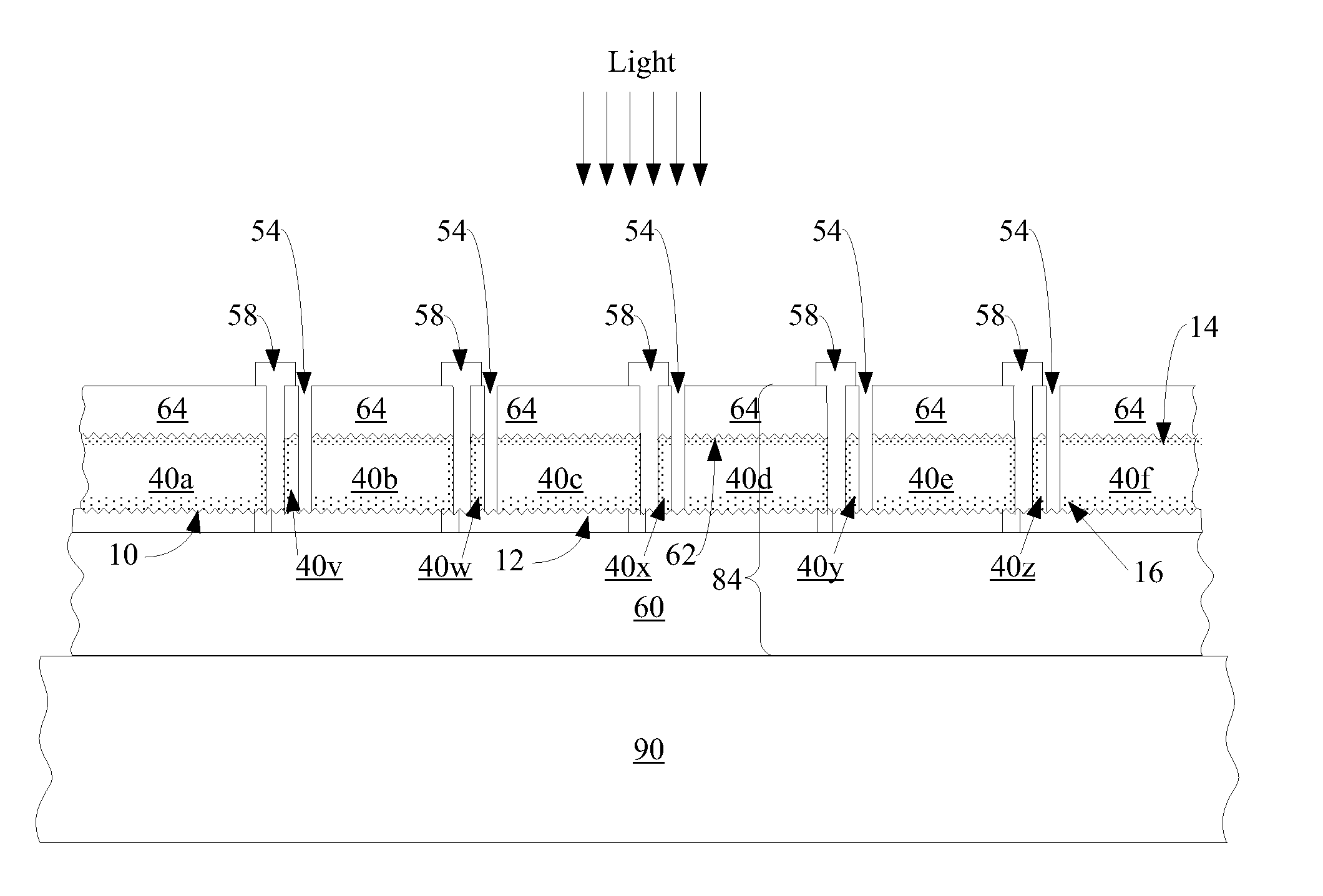
[0055]In the previous example, electrical contact was made to the front surface of the photovoltaic cell with a TCO. In alternative embodiments, metal wiring may be formed to make electrical contact to the front surface of the photovoltaic cell instead. An example of such a photovoltaic cell, comprising a lamina severed into a plurality of segments according to the present invention, will be provided.

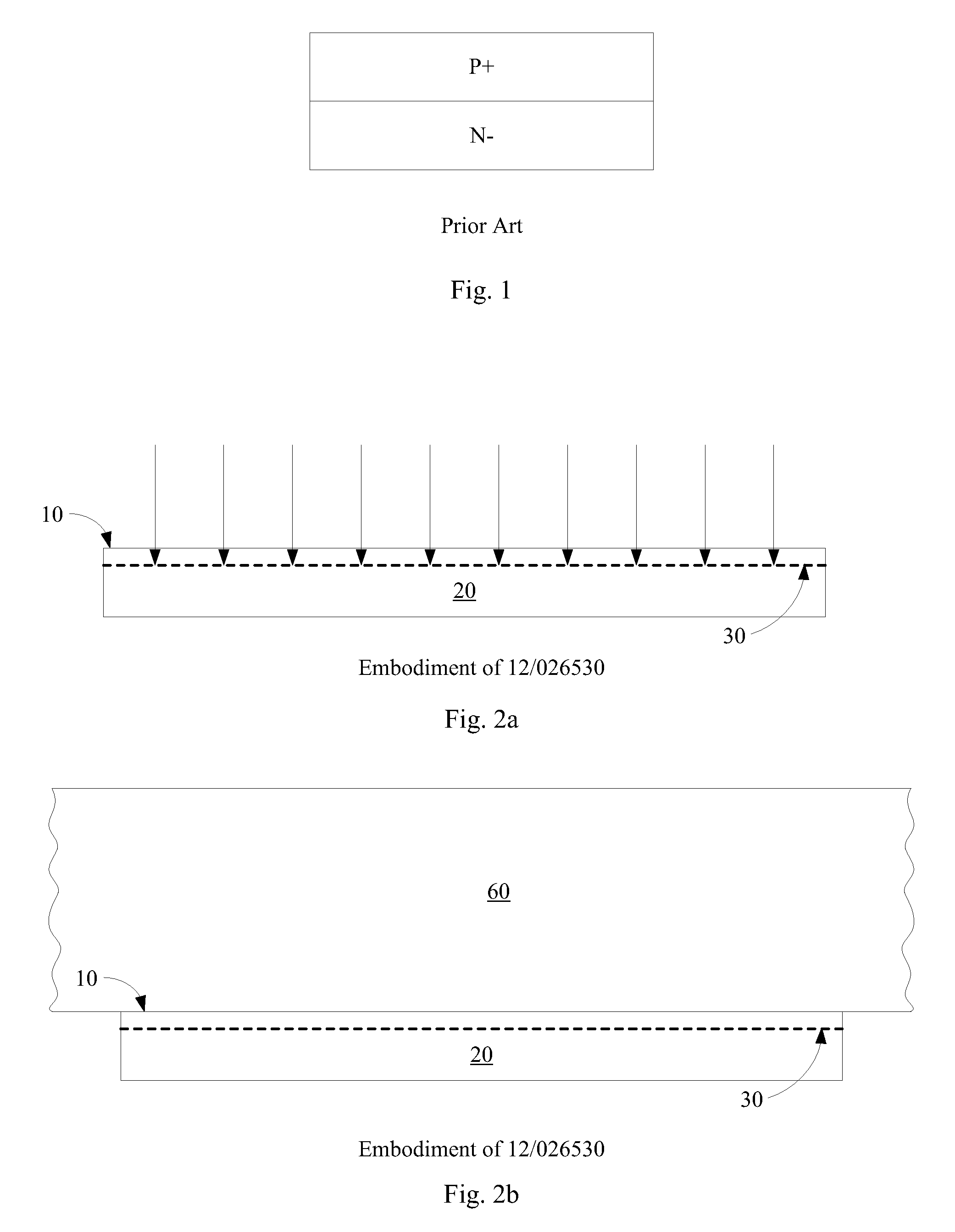
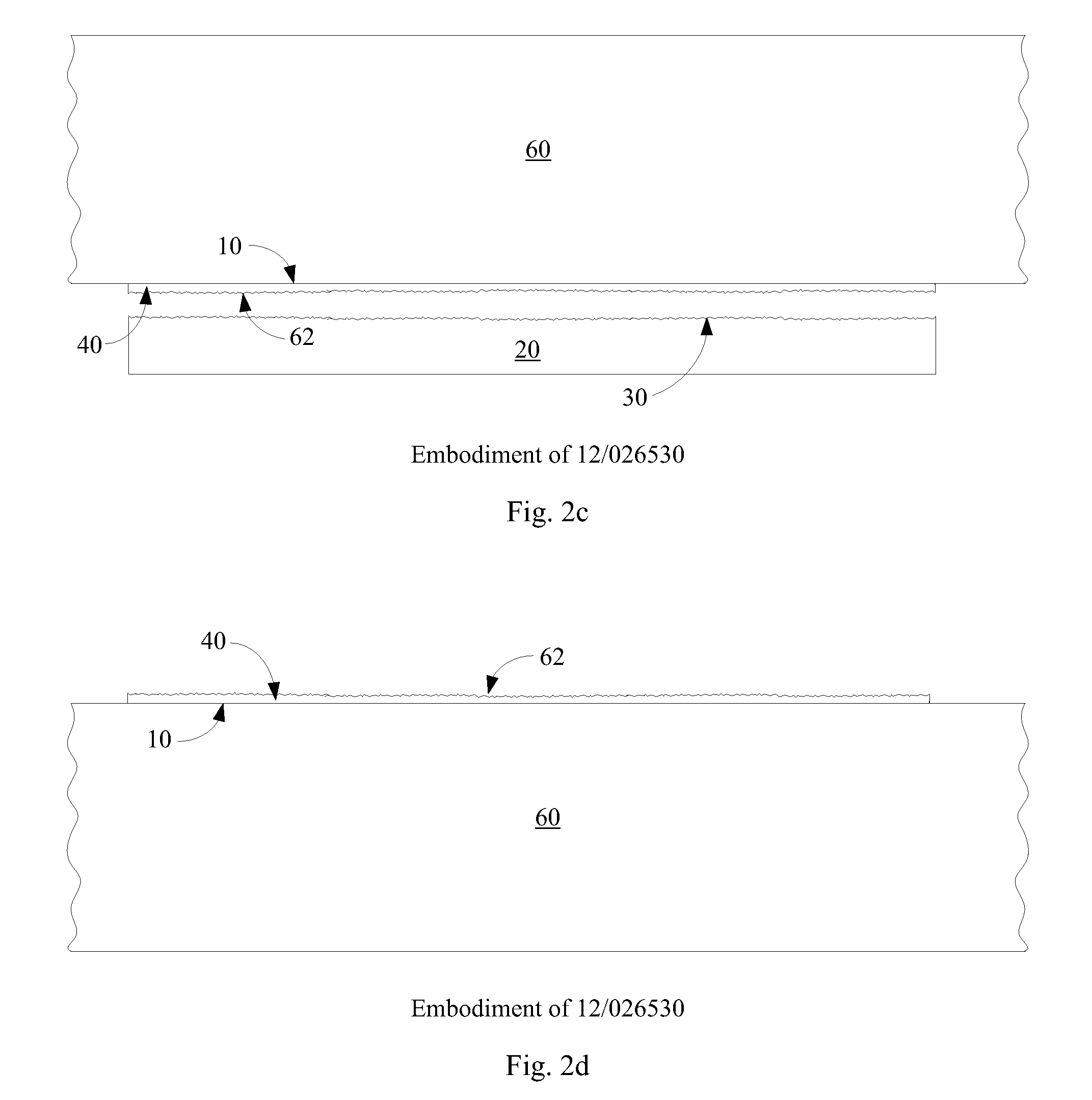
[0056]Referring to FIG. 9a, fabrication begins as in the previous example. A first surface 10 of a lightly n-doped donor wafer (not shown), which may be textured, is doped to form p-doped region 16, then a cleave plane (not shown) is defined in the donor wafer, for example by implanting hydrogen and / or helium ions. Conductive layer 12 is formed on first surface 10, then layer 12 is divided, for example by laser scribing, into a plurality of sections, for example thirty-six sections. For readability, only six sections will be shown. The sections...


PUM


Abstract

A photovoltaic cell can be formed from a thin semiconductor lamina cleaved from a substantially crystalline wafer. Shunts may inadvertently be formed through such a lamina, compromising device performance. By physically severing the lamina into a plurality of segments, the segments of the lamina preferably electrically connected in series, loss of efficiency due to shunt formation may be substantially reduced. In some embodiments, adjacent laminae are connected in series into strings, and the strings are connected in parallel to compensate for the reduction in current caused by severing the lamina into segments.

Description

RELATED APPLICATIONS[0001]This application is related to Hilali et al., U.S. patent application Ser. No. ______, “Photovoltaic Cell Comprising a Thin Lamina Having a Rear Junction and Method of Making,” (attorney docket number TCA-007); and to Hilali et al., U.S. patent application Ser. No. ______, “Photovoltaic Cell Comprising a Thin Lamina Having Low Base Resistivity and Method of Making,” (attorney docket number TCA-001-1), both filed on even date herewith and owned by the assignee of the present application, and both hereby incorporated by reference.[0002]This application is also related to Herner et al., U.S. patent application Ser. No. ______, “Method to Mitigate Shunt Formation in a Photovoltaic Cell Comprising a Thin Lamina,” (attorney docket number TCA-006.y), filed on even date herewith, owned by the assignee of the present application, and hereby incorporated by reference.BACKGROUND OF THE INVENTION[0003]The invention relates to a method to mitigate the loss of efficiency...

Claims


Application Information

Patent Timeline
IPC IPC(8): H01L31/042H01L31/18
CPCH01L31/042H01L31/18H01L31/046H01L31/1892Y02E10/50H01L31/186Y02P70/50
Inventor HERNER, S. BRADPETTI, CHRISTOPHER J.
Owner GTAT CORPORATION
Features
  • R&D
  • Intellectual Property
  • Life Sciences
  • Materials
  • Tech Scout
  • Unparalleled Data Quality
  • Higher Quality Content
  • 60% Fewer Hallucinations
Learn More