Light-emitting module

a technology of light-emitting modules and led chips, which is applied in the direction of light-emitting devices, semiconductor devices for light sources, light-emitting devices, etc., can solve the problems of cracks in the electrical insulating layer, leakage current generation, and the inability to allow the led chip to emit light, etc., to achieve high light stability, maintain heat dissipation, and high heat resistance

Inactive Publication Date: 2010-02-11
PANASONIC CORP
View PDF8 Cites 26 Cited by
  • Summary
  • Abstract
  • Description
  • Claims
  • Application Information

AI Technical Summary

Benefits of technology

[0004]The present invention solves the above-mentioned conventional problem, and its object is to provide a light-emitting module that is capable of maintaining heat dissipation and has high heat resistance and high light stability.

Problems solved by technology

However, according to this heat-dissipating means, the organic material constituting the electrical insulating layer is degraded due to the heat and light generated by the LED chip, with the result that cracks may be generated in the electrical insulating layer.
In the case where cracks are generated in the electrical insulating layer, a leakage current is generated via the cracks when the LED chip is supplied with electricity.
Therefore, it may become impossible to allow the LED chip to emit light.

Method used


Image

  • Light-emitting module
  • Light-emitting module
  • Light-emitting module

Examples


embodiment 1

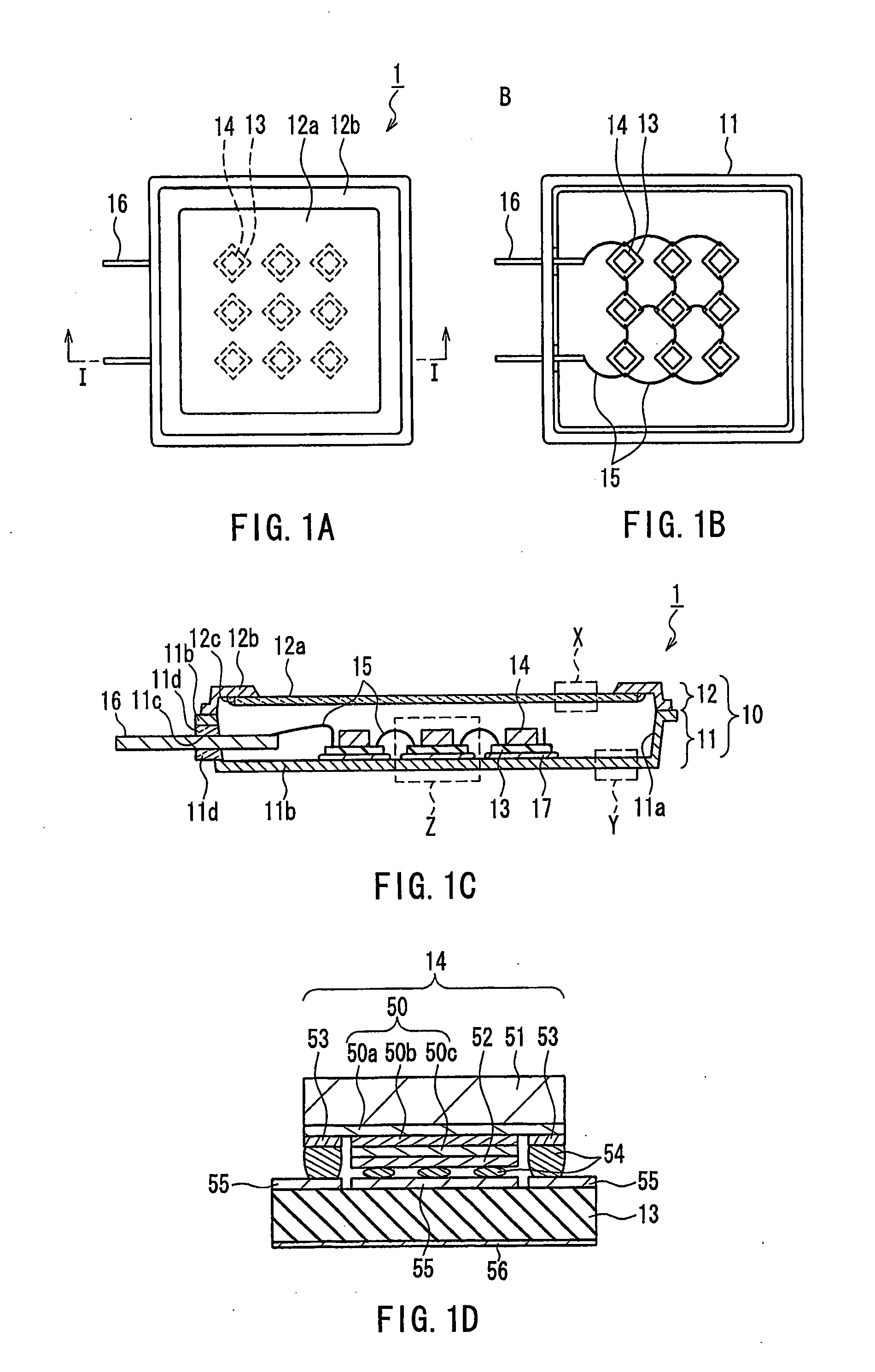
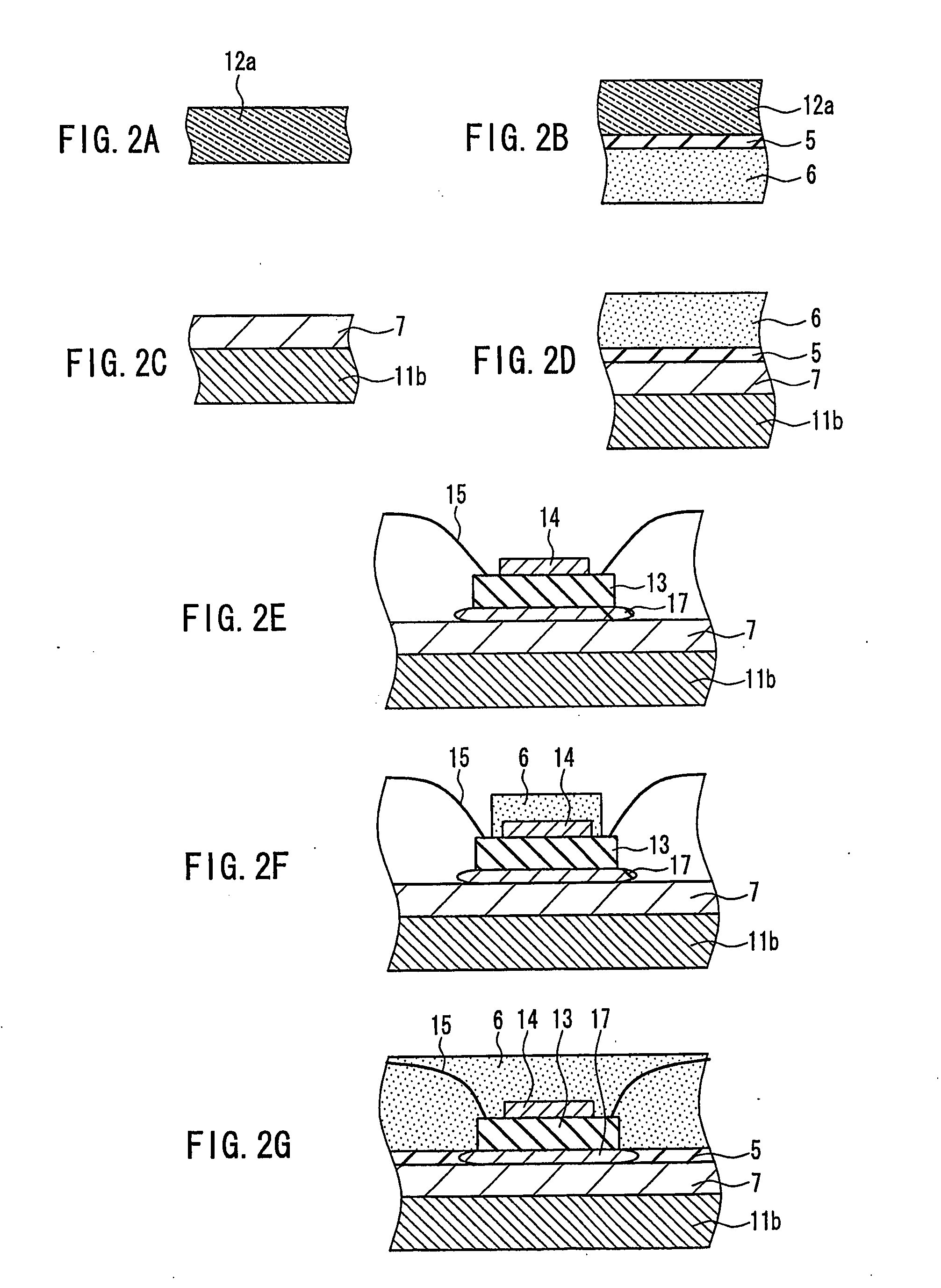
[0032]First, a light-emitting module according to Embodiment 1 of the present invention will be described with reference to the drawings. FIGS. 1A to 1D are views illustrating the light-emitting module according to Embodiment 1. Among them, FIG. 1A is a top view of the light-emitting module according to Embodiment 1, FIG. 1B is a top view showing a state where a cap of the light-emitting module shown in FIG. 1A is removed, FIG. 1C is a cross-sectional view taken along a line I-I in FIG. 1A, and FIG. 1D is an enlarged cross-sectional view of an LED chip and a base board used in the light-emitting module shown in FIG. 1C.

[0033]As shown in FIG. 1C, the light-emitting module 1 according to Embodiment 1 includes a package 10 having a base 11 with a concave portion 11a, and a cap 12 connected to the base 11. The base 11 may be connected to the cap 12, for example, by performing seam welding (welding using a pulse current of about several amperes) under the condition that outer edges of th...

embodiment 2

[0053]Next, a light-emitting module according to Embodiment 2 of the present invention will be described with reference to the drawings. FIGS. 4A to 4C are views illustrating a light-emitting module according to Embodiment 2. Among them, FIG. 4A is a top view of the light-emitting module according to Embodiment 2; FIG. 4B is a top view showing a state where a cap of the light-emitting module shown in FIG. 4A is removed; and FIG. 4C is a cross-sectional view taken along a line II-II in FIG. 4A. In FIGS. 4A to 4C, the same constituent elements as those in FIGS. 1A to 1D are denoted with the same reference numerals as those therein, and the description thereof will be omitted.

[0054]As shown in FIGS. 4A to 4C, a light-emitting module 2 according to Embodiment 2 is different from the light-emitting module 1 (see FIGS. 1A to 1D) according to Embodiment 1, in the connection state of the LED chips 14 and the number of the terminal portions 16. Furthermore, the concave portions 11a (see FIG....

embodiment 3

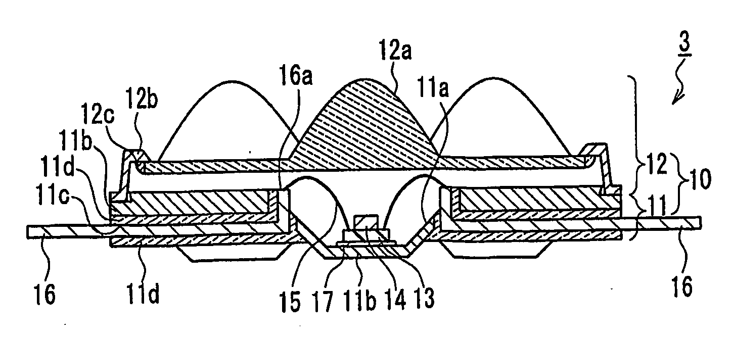
[0055]Next, a light-emitting module according to Embodiment 3 of the present invention will be described with reference to the drawings. FIGS. 5A to 5C are views illustrating the light-emitting module according to Embodiment 3. Among them, FIG. 5A is a top view of the light-emitting module according to Embodiment 3; FIG. 5B is a top view showing a state where a cap of the light-emitting module shown in FIG. 5A is removed; and FIG. 5C is a cross-sectional view taken along a line III-III in FIG. 5A. In FIGS. 5A to 5C, the same constituent elements as those in FIGS. 4A to 4C are denoted with the same reference numerals as those therein, and the description thereof will be omitted.

[0056]As shown in FIGS. 5A to 5C, a light-emitting module 3 according to Embodiment 3 is different from the light-emitting module 2 (see FIGS. 4A to 4C) according to Embodiment 2, in the number of the LED chips 14, the arrangement state of the LED chips 14, the connection state of the LED chips 14, and the sha...


PUM


Abstract

A light-emitting module (1) includes: a package (10); a base board (13) and a semiconductor multi-layered film (50) accommodated in the package (10); and a plurality of terminal portions (16) for supplying electricity to the semiconductor multi-layered film (50), wherein the package (10) includes a metallic support portion (11b) supporting the base board (13), a plurality of through-holes (11c) for insertion of the respective terminal portions (16), an insulating member (11d) keeping electrical insulation between the metallic support portion (11b) and the terminal portions (16), and between the respective terminal portions (16), and a window portion (12a); the base board (13) is made of an inorganic heat-dissipating material that keeps electrical insulation between the semiconductor multi-layered film (50) and the metallic support portion (11b); and one opening of each of the through-holes (11c) is provided on a side surface of the package (10). Because of this, a light-emitting module is provided, which can keep heat dissipation and has high heat resistance and light stability.

Description

TECHNICAL FIELD[0001]The present invention relates to a light-emitting module.BACKGROUND ART[0002]A light-emitting diode (LED) chip including a semiconductor multi-layered film is used for a light source for a backlight of liquid crystal, an indicator such as a meter, a light source for a display, a light source for a read sensor, or the like. In particular, recently, owing to the increase in the optical output of an LED chip and the decrease in a wavelength of light taken out from the LED chip, it is considered to apply the LED chip as an illumination light source. For example, JP 2003-124528 A proposes a light-emitting module capable of realizing high optical output by mounting a number of LED chips on a card-shaped substrate at high density.[0003]The LED chip generates a great amount of heat during use, so that some heat-dissipating means generally is used when applying the LED chip to a light-emitting module. For example, in the light-emitting module in the above-mentioned JP 20...

Claims


Application Information

Patent Timeline
Patent Type & Authority Applications(United States)
IPC IPC(8): H01L33/00H01L33/32H01L33/50H01L33/56H01L33/60H01L33/62H01L33/64
CPCF21K9/00H01L25/0753H01L33/483H01L33/641H01L2224/48137H01L2224/48091H01L2924/00H01L2924/00014
Inventor NAGAI, HIDEO
Owner PANASONIC CORP
Why Eureka
Try Eureka