Eureka AIR delivers breakthrough ideas for toughest innovation challenges, trusted by R&D personnel around the world.

Flash memory control apparatus having signal-converting module

Inactive Publication Date: 2010-02-11
GENESYS LOGIC INC
View PDF2 Cites 9 Cited by
  • Summary
  • Abstract
  • Description
  • Claims
  • Application Information

AI Technical Summary

Benefits of technology

[0005]The primary controller generates a first set of control signals based on a first control interface. The first set of control signals further includes a reading enable signal and a writing enable signal. The signal-converting module receives the reading enable signal and the writing enable signal from the primary controller. The signal-converting module further converts both the reading enable signal and the writing enable signal into a writing/reading signal based on a second control interface. For example, while the writing/reading signal is high level, the data are sent to the flash memory. Conversely, while the writing/reading signal is high level, the data are outputted from the flash memory.
[0006]The first set of control signals based on the first control interface includes a command latch enable signal (SCLE), a chip enable signal (/SCE), a write enable signal (/SWE), an address latch enable signal (SALE), a read enable signal (/SRE), an input/output (I/Ox) signal, a write protecting signal (/WP), and a ready/busy (R/B) status signal. The second set of control signals based on the second control interface includes a command latch enable signal (SCLE), a chip enable signal (/SCE), a writing/reading signal /(W/R), an address latch enable signal (SALE), a data strobe signal (DQS), a DQx signal, a clock signal (CLK), a write protecting signal (IWP), and a ready/busy (R/B) status signal. In the present invention, “asynchronous” indicates that the data are latched with /SWE signal during the writing procedure and the data are latched with /SRE signal during the reading procedure. “Synchronous represents when the strobe signal (DQS) is forwarded the data to indicate when the data should be latched.
[0007]The command latch enable signal (SCLE) is one o

Problems solved by technology

However, the interface specification of the conventional NAND flash memory cannot be compatible to the interface of the ONFI flash memory.
Therefore, these products adopting the old NAND flash memory need to be re-designed so as to meet the standard protocol of the interface of ONFI flash memory, thereby resulting in no cost-effectiveness.

Method used


Image

  • Flash memory control apparatus having signal-converting module
  • Flash memory control apparatus having signal-converting module
  • Flash memory control apparatus having signal-converting module

Examples


Embodiment Construction

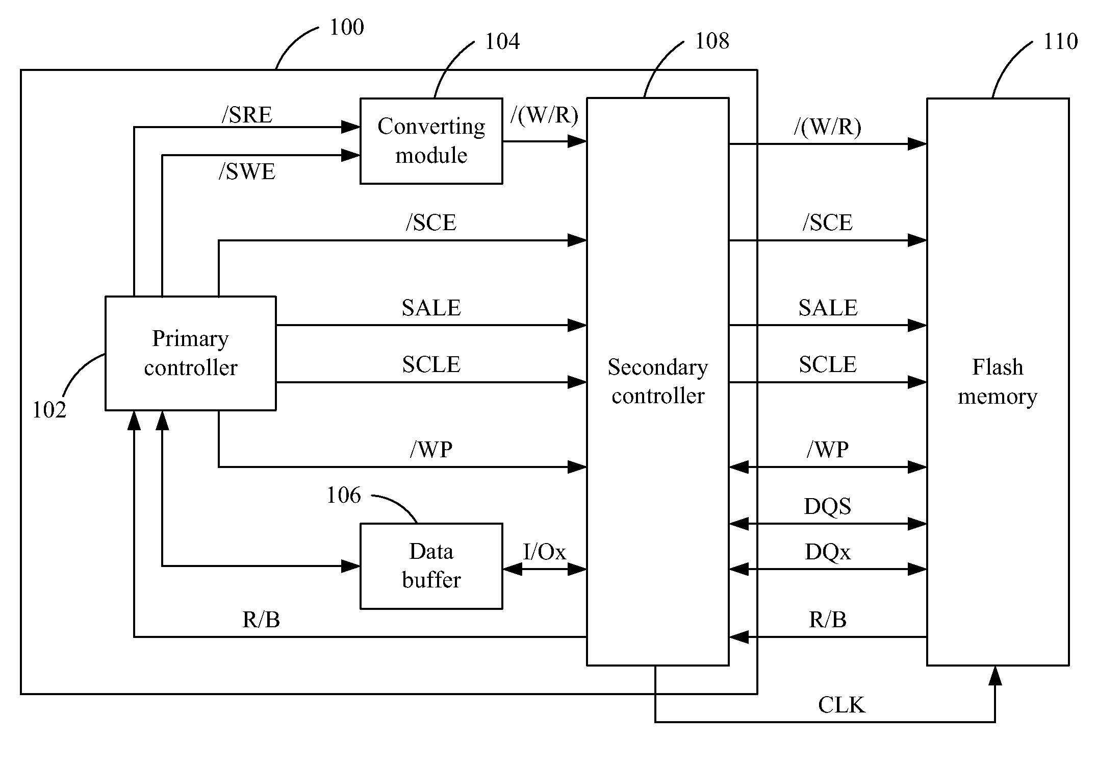
[0015]FIG. 1 is a schematic block diagram of a flash memory control apparatus 100 having a signal-converting module 104 according to one embodiment of the present invention. The flash memory control apparatus 100 includes a primary controller 102, a signal-converting module 104, a data buffer 106, and a secondary controller 108. The flash memory control apparatus 100 is used to control a flash memory 110. The signal-converting module 104 is coupling the primary controller 102 to the secondary controller 108 therebetween. The data buffer 106 is coupling the primary controller 102 to the secondary controller 108 therebetween. The secondary controller 108 is coupled to the flash memory 110.

[0016]The primary controller 102 generates a first set of control signals based on a first control interface. The first set of control signals further includes a reading enable signal and a writing enable signal. The signal-converting module 104 receives the reading enable signal and the writing enab...


PUM


Abstract

A flash memory control apparatus having a signal-converting module is described. The signal-converting module includes a primary controller, a signal-converting module, a data buffer, and a secondary controller. The primary controller generates a plurality of control signals based on a first control interface. The signal-converting module receiving a reading enable signal and a writing enable signal of the control signals and converts the reading enable signal and the writing enable signal into a writing / reading signal based on a second control interface. The data buffer stores the data from the primary controller according to the first control interface and stores the data from the flash memory according to the second control interface. The secondary controller transmits the writing / reading signal, a clock signal and a data strobe signal to the flash memory based on the second control interface.

Description

FIELD OF THE INVENTION [0001]The present invention relates to a memory apparatus, and more particularly relates to a flash memory control apparatus having a signal-converting module which is applicable to NAND (Not AND) flash memory.BACKGROUND OF THE INVENTION [0002]With the rapid development of flash memory, a variety of flash memory interface specifications, such as NAND (Not AND) flash, are widely utilized. For performance improvement of the NAND flash memory, one kind of flash interface, e.g. open NAND flash interface (ONFI) standard protocol, is thus established. However, the interface specification of the conventional NAND flash memory cannot be compatible to the interface of the ONFI flash memory. Particularly, the pin assignments of the conventional NAND flash memory are different from these of the ONFI flash memory. Generally speaking, the ONFI flash memory only supports the type of on-die controller. Therefore, these products adopting the old NAND flash memory need to be r...

Claims


Application Information

Patent Timeline
IPC IPC(8): G06F12/00
CPCG06F13/1673
Inventor CHEN, JU-PENGHSU, YU-JEN
Owner GENESYS LOGIC INC
Why Eureka
Eureka Blog
Learn More