Method of processing optical device wafer

a processing method and optical device technology, applied in the direction of laser beam welding apparatus, manufacturing tools, welding/soldering/cutting articles, etc., can solve the problems of difficult cutting of sapphire substrate by a cutter, high mohs hardness, and difficult-to-cut materials

Active Publication Date: 2010-02-18
DISCO CORP
View PDF12 Cites 36 Cited by
  • Summary
  • Abstract
  • Description
  • Claims
  • Application Information

AI Technical Summary

Benefits of technology

[0008]Accordingly, it is an object of the present invention to provide a method of processing an optical device wafer by ...

Problems solved by technology

As a method for dividing the optical device wafer along the streets, a method of cutting the optical device wafer by a cutting blade rotated at high speed has been attempted, but it is difficult to cut the sapphire substrate ...

Method used


Image

  • Method of processing optical device wafer
  • Method of processing optical device wafer
  • Method of processing optical device wafer

Examples


Embodiment Construction

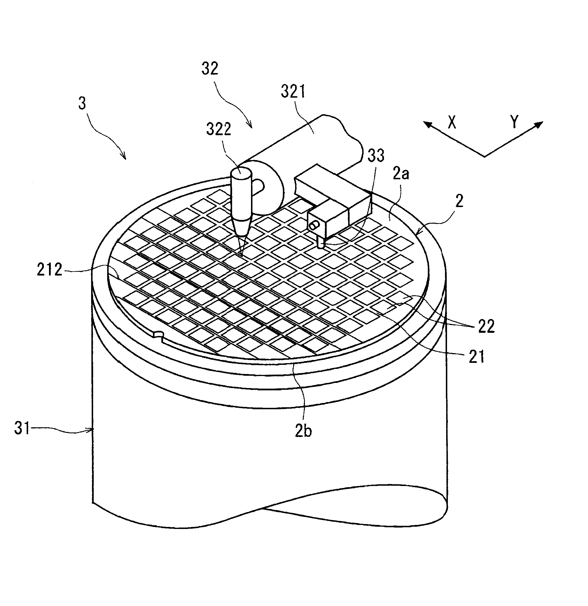
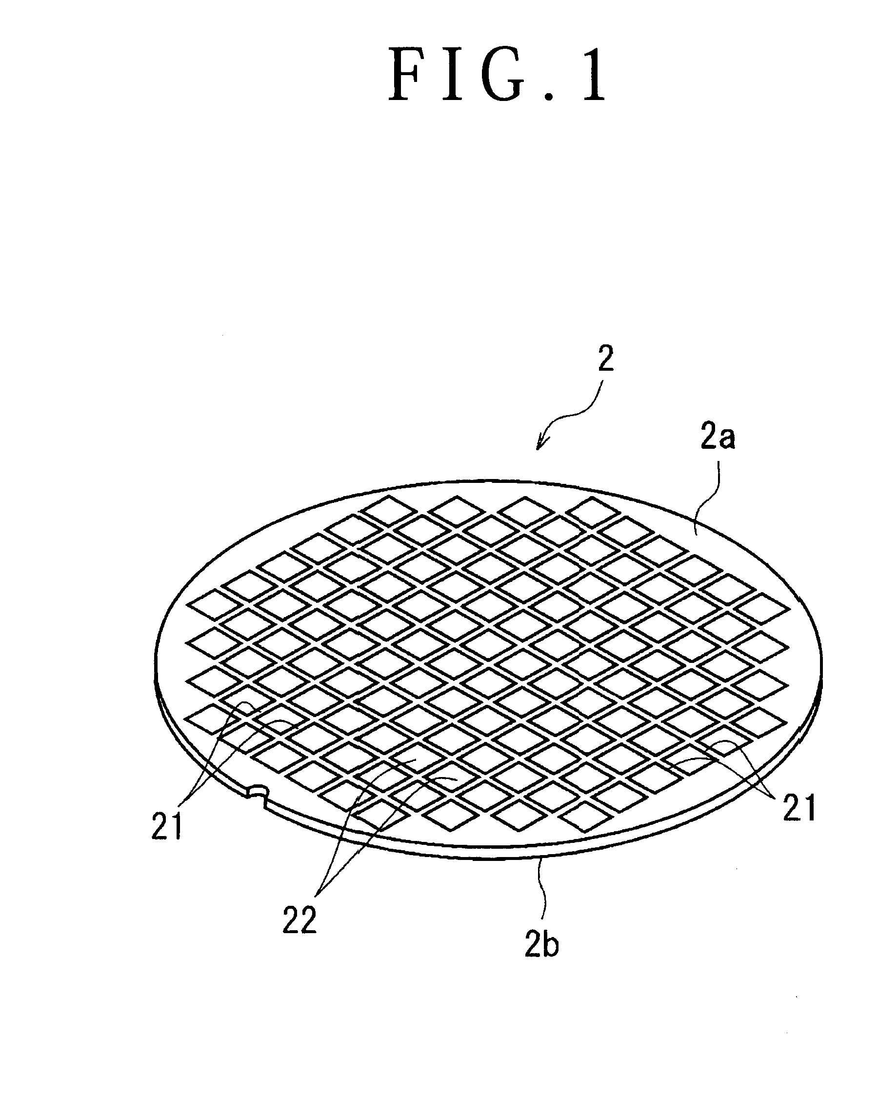
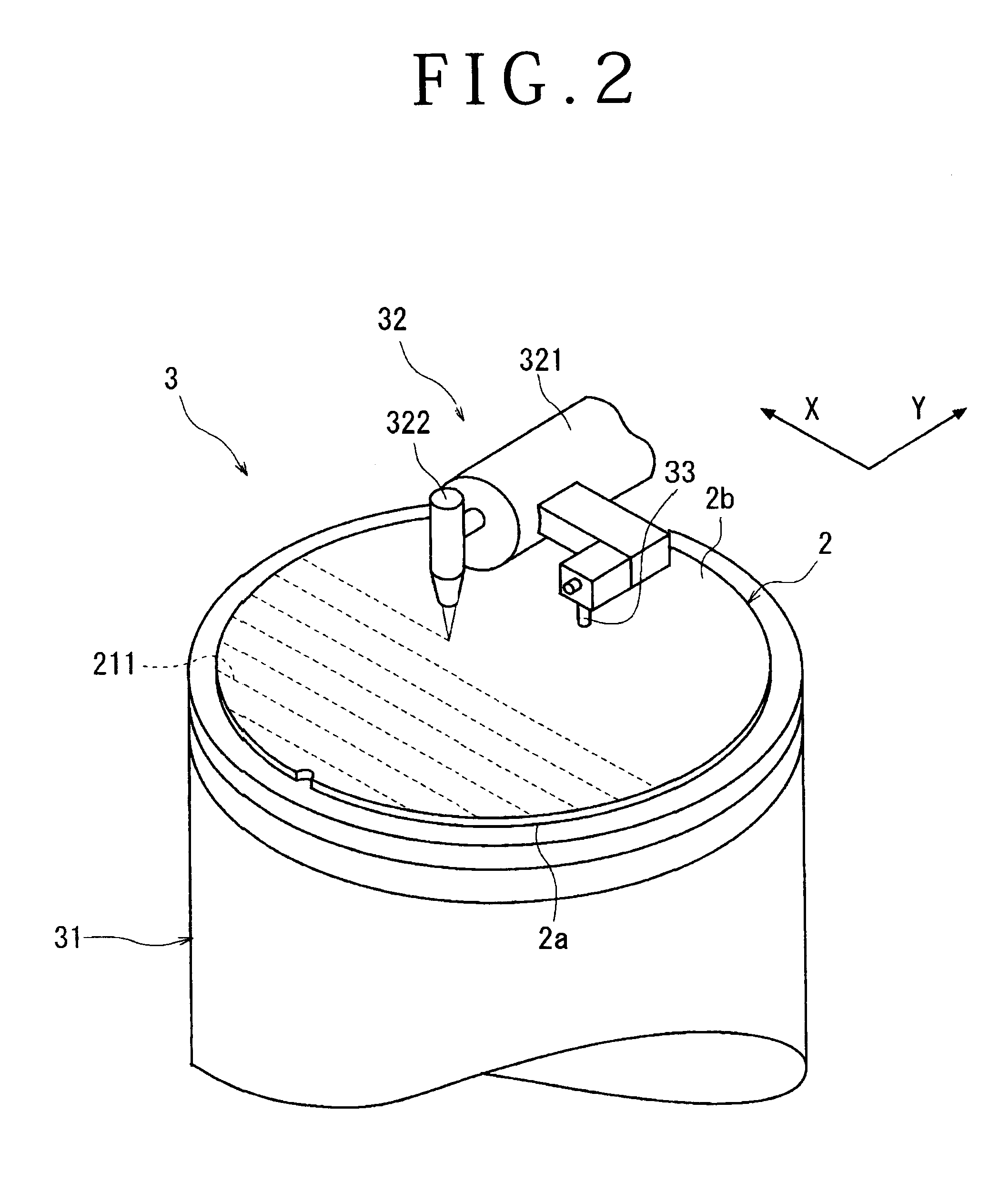
[0029]Now, preferred embodiments of the method of processing an optical device wafer according to the present invention will be described in detail below, referring to the attached drawings. FIG. 1 shows an optical device wafer 2 to be divided by the method of processing an optical device wafer according to the invention. The optical device wafer 2 shown in FIG. 1 has a configuration in which a plurality of regions are demarcated by streets 21 formed in a grid pattern on a face-side surface 2a of a sapphire substrate which, for example, has a diameter of 100 mm and a thickness of 425 μm, and a plurality of optical devices 22 such as light emitting diodes are formed in the demarcated regions.

[0030]A first embodiment of the method of processing an optical device wafer for dividing the above-mentioned optical device wafer 2 along the streets 21 into the individual optical devices 22 will be described, referring to FIGS. 2 to 12. In order to divide the optical device wafer 2 along the s...


PUM

PropertyMeasurementUnit
Frequencyaaaaaaaaaa
Nanoscale particle sizeaaaaaaaaaa

Abstract

A method of dividing an optical device wafer includes: a laser beam processing step of performing laser beam processing on the face side of an optical device wafer so as to form breakage starting points along streets; a protective plate bonding step of bonding the face side of the optical device wafer to a surface of a highly rigid protective plate with a bonding agent permitting peeling; a back side grinding step of grinding the back side of the optical device wafer so as to form the optical device wafer to a finished thickness of optical devices; a dicing tape adhering step of adhering the back-side surface of the optical device wafer to a dicing tape; a cut groove forming step of cutting the protective plate bonded to the optical device wafer along the streets so as to form cut grooves; and a wafer dividing step of exerting an external force on the optical device wafer through the protective plate, so as to break up the optical device wafer along the breakage starting points formed along the streets, thereby dividing the optical device wafer into the individual optical devices.

Description

BACKGROUND OF THE INVENTION[0001]1. Field of the Invention[0002]The present invention relates to a method of processing an optical device wafer by which an optical device wafer having optical devices composed of a gallium nitride compound semiconductor or the like layered in a plurality of regions demarcated by streets formed in a grid pattern on the face-side surface of a substrate such as a sapphire substrate is divided along the streets into the individual optical devices.[0003]2. Description of the Related Art[0004]An optical device wafer in which a plurality of regions are demarcated by planned dividing lines called streets formed in a grid pattern on the face-side surface of a sapphire substrate and optical devices composed of a gallium nitride compound semiconductor or the like are layered in the demarcated regions is divided along the streets into the individual optical devices such as light emitting diodes, which are widely utilized for electric apparatuses. As a method for...

Claims


Application Information

Patent Timeline
IPC IPC(8): H01L21/302B23K26/38H01L33/00H01L33/02
CPCH01L33/0095H01L21/67132H01L21/67092B23K26/4075B23K26/40B23K2103/50H01L33/48H01L21/78
Inventor HOSHINO, HITOSHIYAMAGUCHI, TAKASHI
Owner DISCO CORP
Why Eureka
Try Eureka