Method of manufacturing electronic components having bump

a manufacturing method and electronic component technology, applied in the direction of resistive material coating, final product manufacturing, solid-state devices, etc., can solve the problems of reducing yield, wiring substrate and other electronic components to undergo unsatisfactory connection, and cannot solve, so as to reduce the yield of wiring substrate and other electronic components, suppress the maintenance of passivation film, and improve the flux wet and spread characteristic of the outer peripheral portion of the hump

Inactive Publication Date: 2010-02-25
NEC CORP
View PDF16 Cites 13 Cited by
  • Summary
  • Abstract
  • Description
  • Claims
  • Application Information

AI Technical Summary

Benefits of technology

[0012]The following findings have been obtained: flux within solder paste having passivation film removable action is wetted and spread in bump outer peripheral directions through bump front end portions in contact with the solder paste; even if the front end positions of bumps on the same wiring substrate are not completely flush with each other by warp of the wiring substrate and there is an unevenness etc., of a printing height of the solder paste; for this reason, contact area between the bump front end portions and the solder paste varies every bump; flux is not sufficiently wetted and spread toward bump surface in the case of a bump having a small contact area with solder paste; and a passivation film is maintained at the time of melting. In this invention, a recessed portion is formed from the bump front end portion toward the bump outer periphery. Thus wet and spread characteristic of flux at the outer peripheral portion of the hump is improved thus to have ability to suppress the maintenance of the passivation film. Accordingly, lowering of yield when a wiring substrate is connected to other electronic components can be suppressed.
[0013]Moreover, it has been found that a bump which has come into contact with solder paste once is away from the solder paste by change of warp shape of a wiring substrate followed by temperature elevation in a heating process at the time of performing connection with other components. In the state where the bump is away from the solder paste, even if the bump is melted there does not take place connection with solder paste. Moreover, since supply of flux from the solder paste toward the bump surface is stopped in that state, when flux components existing on the bump surface is exhausted or volatilized, a passivation film would be formed on the bump surface for a second time. Thereafter, even if there is returned to the state in contact with the solder paste for a second time, there may not take place the case where connection is made by a passivation film which has been re-formed on the surface. In the present invention, since a recessed portion is formed from a bump front end portion toward a bump outer periphery, solder paste and the bump front end portion are caused to be contact with each other so that much flux held on the inner wall surface of the recessed portion. Thereafter, even if there results in the case where the bump and the solder paste are away from each other, since much flux is held on the bump surface, it is possible to suppress reformation of a passivation film onto the bump surface due to exhaust of flux components. Accordingly, lowering of yield when wiring substrate is connected to other electronic components is suppressed.

Problems solved by technology

However, the inventor has found out from the technologies described in the above-mentioned literatures that the following problems cannot be solved.
However, there is a possibility that even if the bump is heated so that the temperature becomes equal to melting point or more, the bump is not sufficiently wetted to terminals of other substrate to thereby allow the wiring substrate and other electronic components to undergo unsatisfactory connection so that the yield is lowered.
However, there takes place the problem that when a closed recessed portion with respect to an outer periphery exists at a contact surface between one terminal and the other terminal in forming such uneven portions, flux is accumulated at that portion so that the flux is not sufficiently delivered up to the outer periphery.

Method used


Image

  • Method of manufacturing electronic components having bump
  • Method of manufacturing electronic components having bump
  • Method of manufacturing electronic components having bump

Examples


Embodiment Construction

[0026]The invention will be now described herein with reference to illustrative embodiments. Those skilled in the art will recognize that many alternative embodiments can be accomplished using the teachings of the present invention and that the invention is not limited to the embodiments illustrated for explanatory purpose.

x Preferred embodiments of the present invention will now be described with reference to the attached drawings. In all drawings, similar reference numerals are respectively attached to similar components, and the explanation thereof will be omitted as occasion demanded.

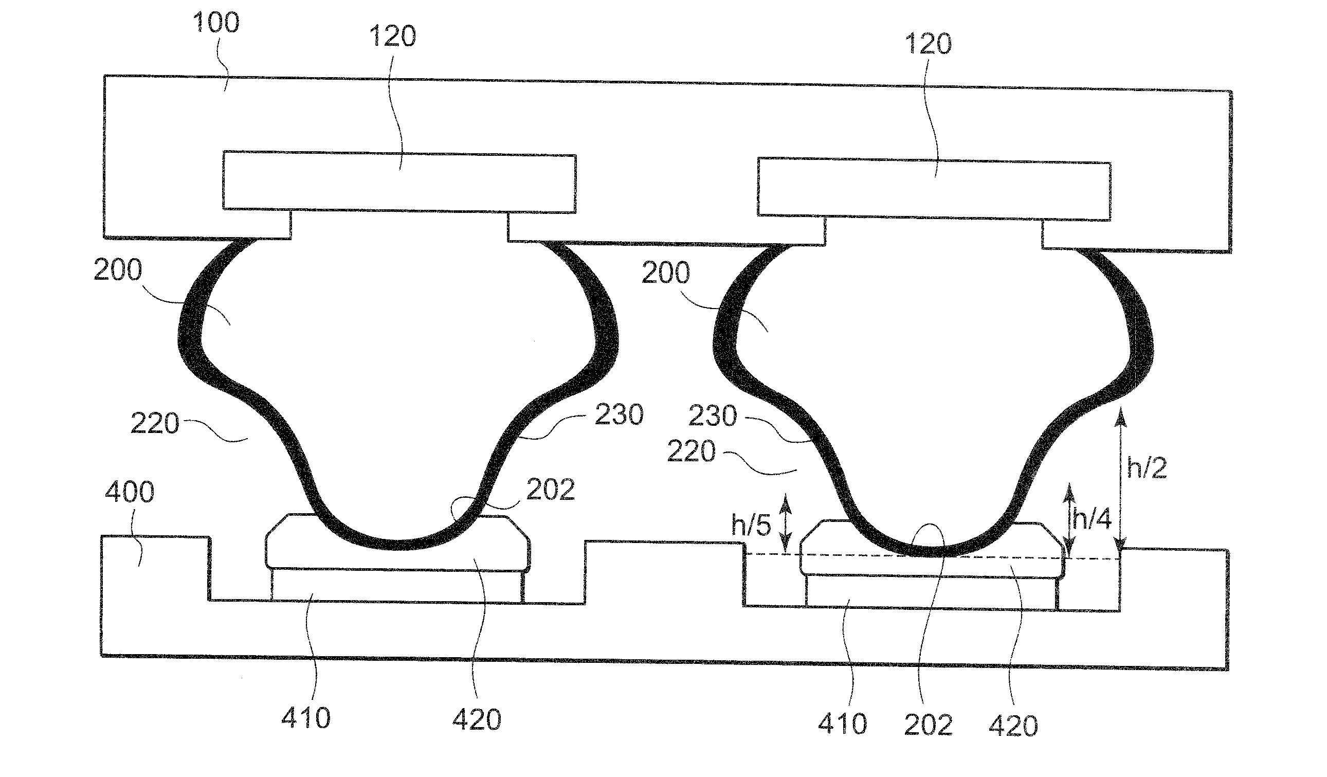
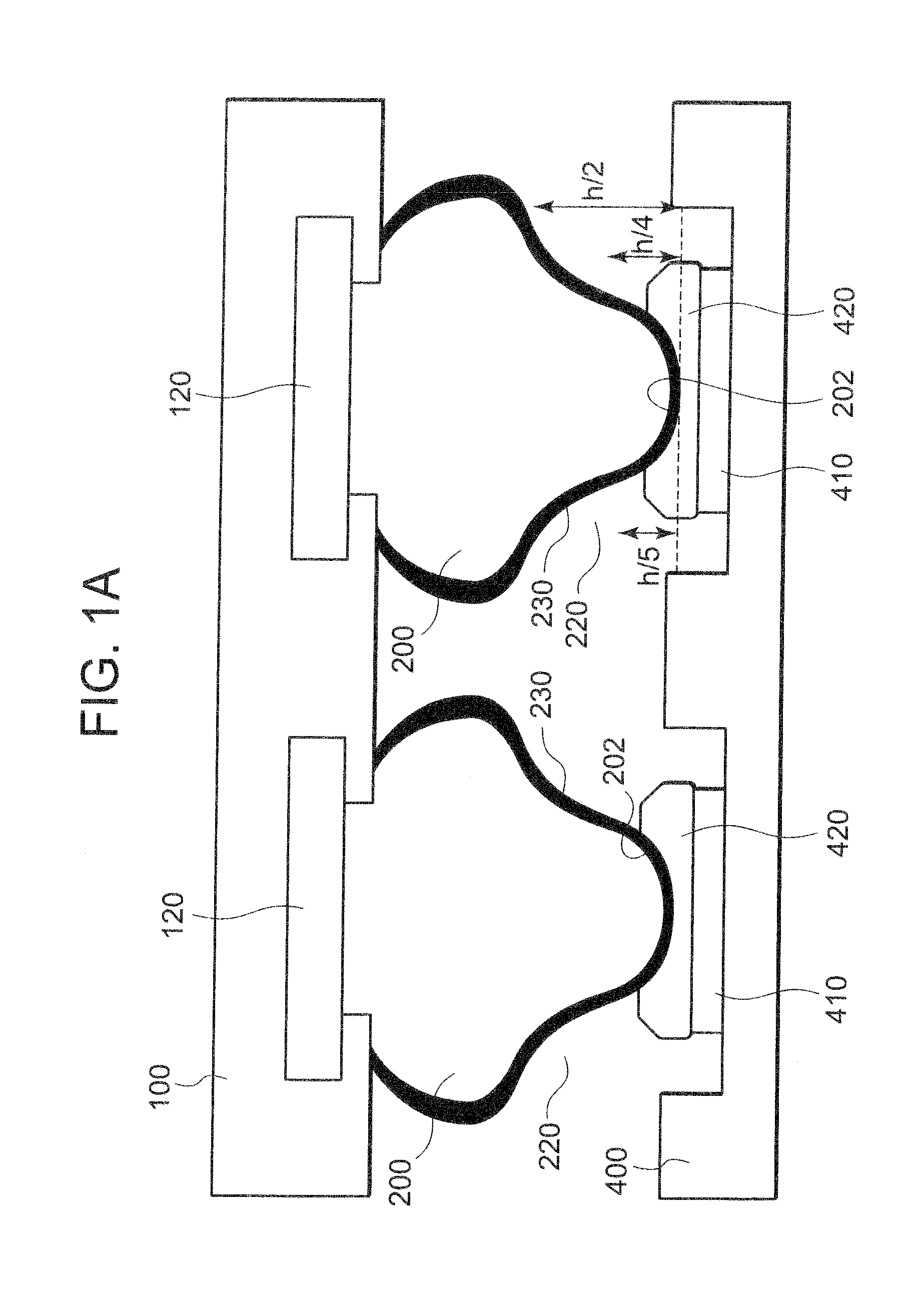
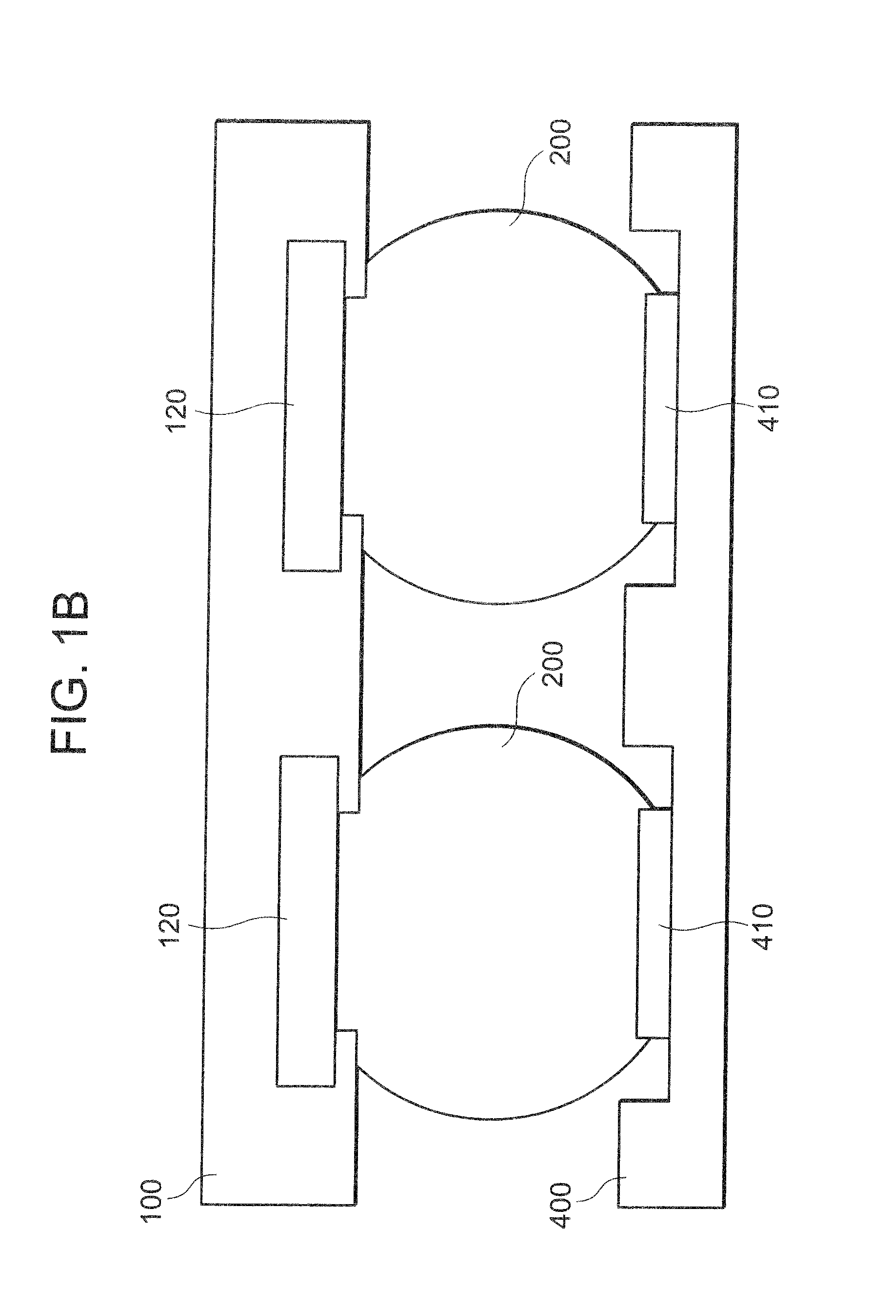
[0027]FIGS. 1A and 1B are cross sectional views of an electronic component relating to the present invention. FIG. 1A shows a state where a second wiring substrate 400 has been caused to undergo positioning relative to a first wiring substrate 100 and FIG. 1B is a view showing a state where the second wiring substrate 400 has been caused to undergo positioning thereafter to perform heat treatment so...


PUM

PropertyMeasurementUnit
aspect ratioaaaaaaaaaa
speedaaaaaaaaaa
speedaaaaaaaaaa

Abstract

An electronic component manufacturing method including: a step of mounting a bump formation material on a first wiring substrate 100 to melt the bump formation material to form a bump 200 at the wiring substrate 100; a step of pressing a jig onto the bump 200 to form a recessed portion 220 having a front end portion 202; a step of printing a solder paste 420 onto an electrode 410 of a second wiring substrate 400; a step of performing, on the solder paste 420, positional alignment of the bump 200 on the wiring substrate 100 to allow the front end portion 202 to be in contact with the bump; and a step of heating the wiring substrate 400 on which the wiring substrate 100 is mounted, wherein the recessed portion 220 is formed from the bump front end portion 202 toward an outer periphery 230 in contact with the solder paste 420.

Description

[0001]The present application is filed on the basis of Japanese Patent Application No. 2008-212645.BACKGROUND OF THE INVENTION[0002]The present invention relates to a method of manufacturing electronic components having wiring substrates and bumps and a method of mounting a substrate, and more particularly to a method of manufacturing electronic components having ability to suppress reduction in yield at the time of connection.[0003]As a technology for mounting wiring substrate on which semiconductor chips are mounted onto other substrates such as a mother board, there is provided a technology to provide bumps as an external connection terminal at the wiring substrate to connect the wiring substrate and the other substrate through the bumps.[0004]In Japanese Patent Laid-Open No. 2003-218161, there is disclosed a technology relating to solder bump planarization press-jig for planarizing summit parts of plural solder bumps so that they are flush with each other. In Japanese Patent Lai...

Claims


Application Information

Patent Timeline
Patent Type & Authority Applications(United States)
IPC IPC(8): B23K1/20B05D5/12
CPCH01L21/4853H01L23/49816H01L2224/16H01L2924/01078H01L2924/01019H05K3/3436H05K2203/0195H05K2203/0465H01L2924/01079H01L2224/0554H01L2224/05567H01L2224/05573H01L2924/00014Y02P70/50H01L2224/05599H01L2224/0555H01L2224/0556
Inventor OGAWA, KENTA
Owner NEC CORP
Why Eureka
Try Eureka