Planar antenna and wireless communication apparatus

a wireless communication and antenna technology, applied in the direction of antennas, antenna details, antenna supports/mountings, etc., can solve the problems of the cost of a single antenna is about 20-30 nt presently, and the system manufacture has to spend more human labor and time for assembling the antenna, so as to reduce the material cost and labor cost of assembling, and the effect of reducing the increase of material cost and labor cos

Active Publication Date: 2010-02-25
ASUSTEK COMPUTER INC
View PDF11 Cites 47 Cited by
  • Summary
  • Abstract
  • Description
  • Claims
  • Application Information

AI Technical Summary

Benefits of technology

[0019]In the present invention, the stepped impedance device is used for substituting a through-hole structure in a conventional planar antenna. Moreover, the coupling device is used for coupling the signal received by the planar antenna to the lead wire crossing the slot line of the metal layer. Therefore, compared to the conventional technique, the planar antenna of the present i

Problems solved by technology

However, a cost of a single antenna is about 20-30 NT presently, so that 100-150 NT have to be spent for the antenna cost of the wireless communication apparatus.
Moreover, as a number of the inbuilt antenna increases, a system manufacture has to sp

Method used


Image

  • Planar antenna and wireless communication apparatus
  • Planar antenna and wireless communication apparatus
  • Planar antenna and wireless communication apparatus

Examples


Embodiment Construction

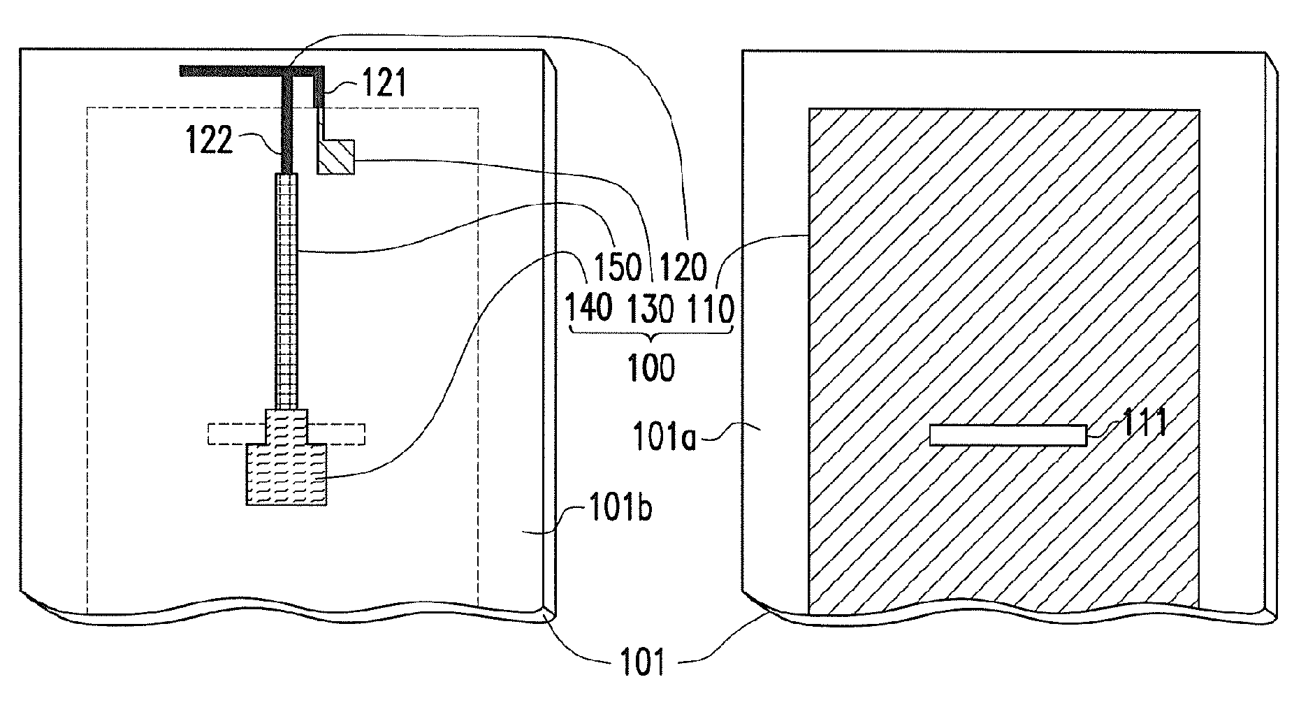
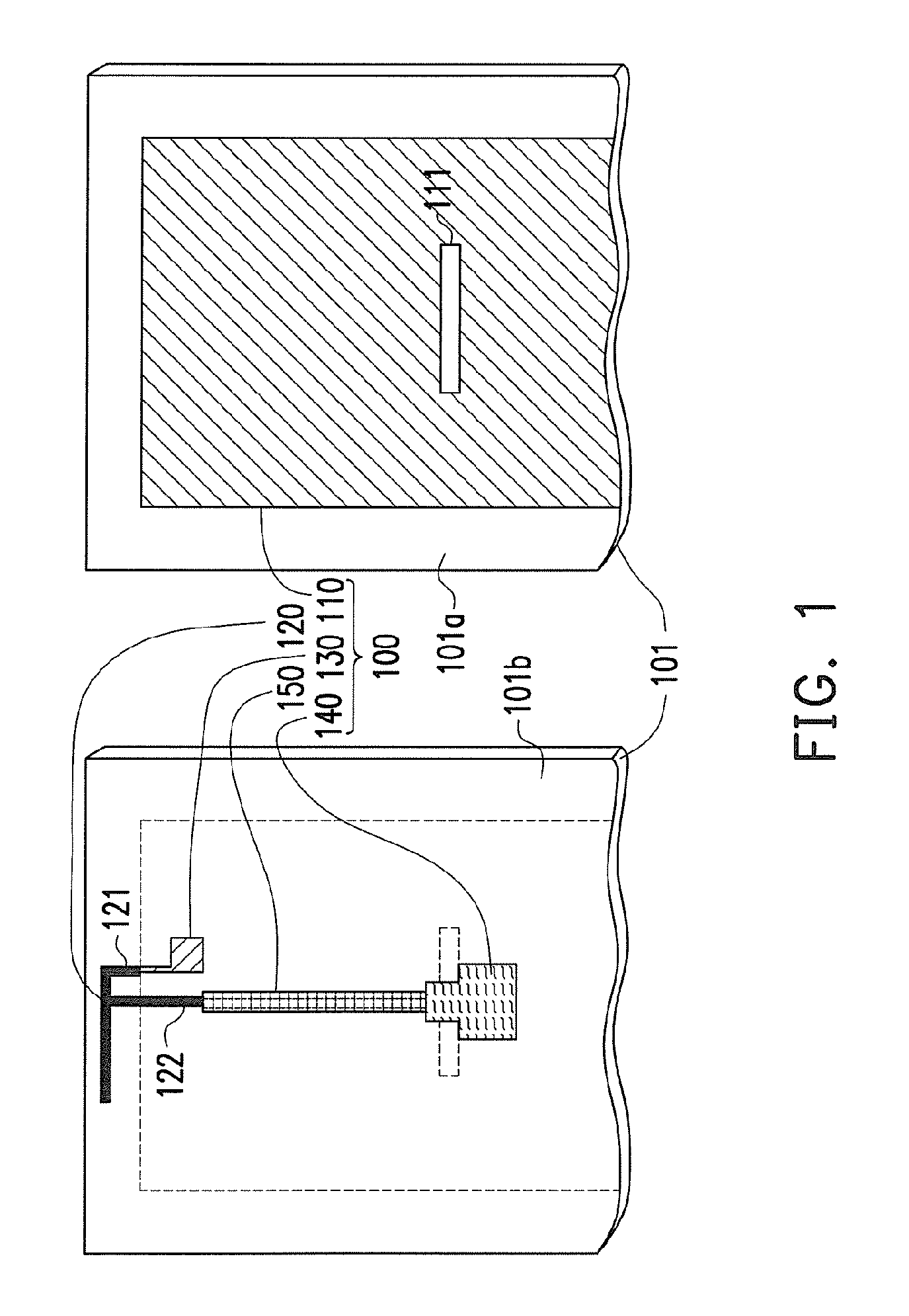
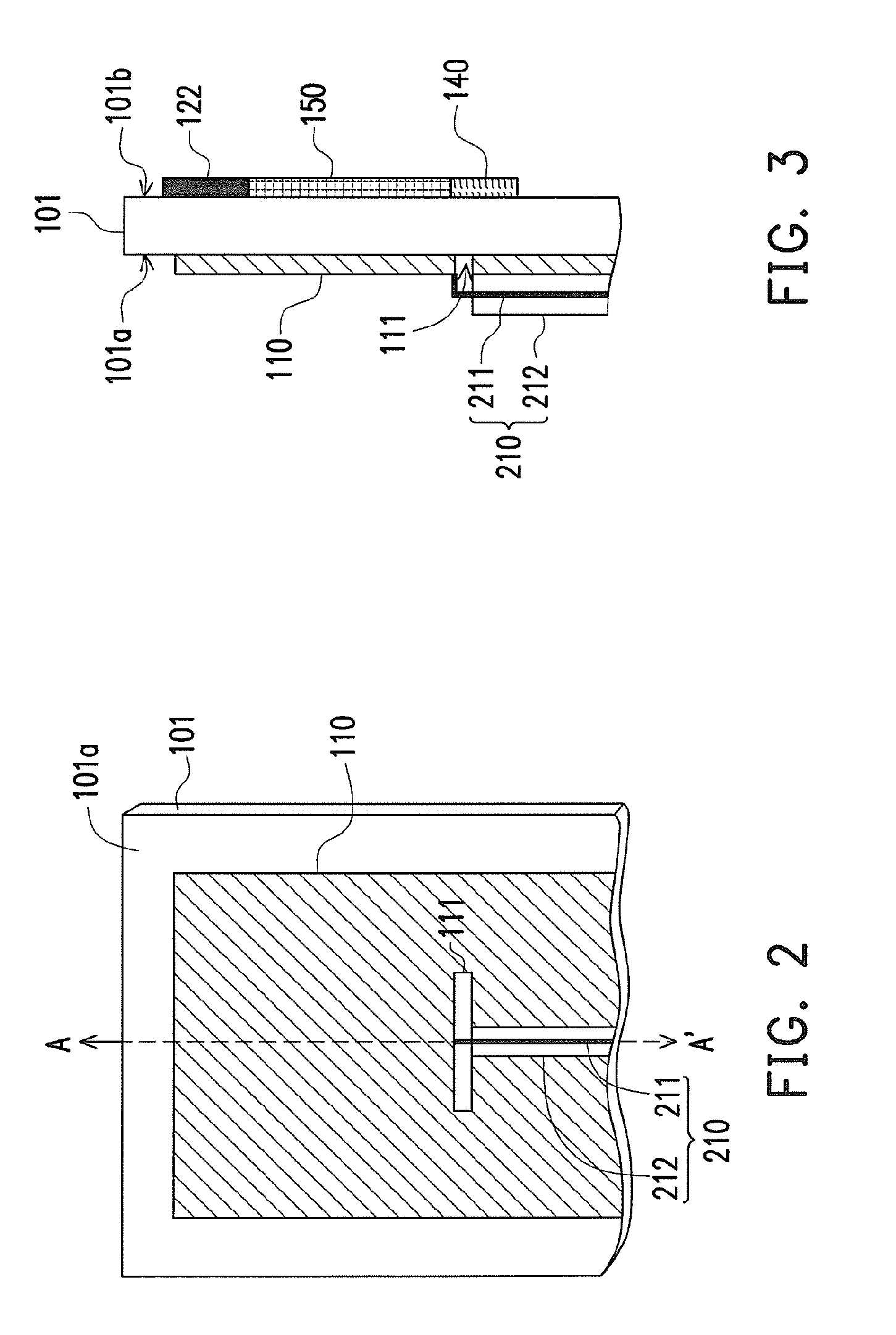
[0036]FIG. 1 is a schematic diagram illustrating a structure of a planar antenna according to an embodiment of the present invention. The planar antenna 100 is disposed on a plate 101, and the plate 101 has a first surface 101a and a second surface 101b.

[0037]It should be noted that in the present embodiment, the plate 101 can be a printed circuit board (PCB), and the first surface 101a is parallel to the second surface 101b. However, those skilled in the art can also apply the planar antenna 100 to any plate having two surfaces according to actual design requirements. In other words, though the present embodiment provides a possible pattern of the plate 101, it is not used for limiting the present invention.

[0038]Referring to FIG. 1 again, the planar antenna 100 includes a metal layer 110, an antenna body 120, a stepped impedance device 130, a coupling device 140 and a matching device 150. Wherein, the metal layer 110 is disposed on the first surface 101a and has a slot line 111 f...


PUM


Abstract

A planar antenna disposed on a plate having a first surface and a second surface is provided. The planar antenna includes a metal layer, an antenna body, a stepped impedance device, a coupling device and a matching device. The metal layer is disposed on the first surface and has a slot line exposing the first surface. The antenna body, the stepped impedance device, the coupling device and the matching device are disposed on the second surface. The antenna body is corresponding to a surrounding of the metal layer except a feed end thereof, the stepped impedance device and the matching device are corresponding to the metal layer, and the coupling device is corresponding to the slot line. The matching device is coupled between the coupling device and the feed end. The stepped impedance device has a transmission zero in a radio frequency band operated by the antenna body.

Description

CROSS-REFERENCE TO RELATED APPLICATION[0001]This application claims the priority benefit of Taiwan application serial no. 97131819, filed Aug. 20, 2008. The entirety of the above-mentioned patent application is hereby incorporated by reference herein and made a part of specification.BACKGROUND OF THE INVENTION[0002]1. Field of the Invention[0003]The present invention relates to a planar antenna and a wireless communication apparatus. More particularly, the present invention relates to a planar antenna without a through-hole structure and a wireless communication apparatus[0004]2. Description of Related Art[0005]With development of hardware device and technique for wireless transmission, a multi input multi output (MIMO) technique has become an important indicator for a high efficiency wireless communication technique, and gradually becomes a main stream for future wireless communication. Different to a conventional design of a single antenna, the MIMO technique applies multi antenna...

Claims


Application Information

Patent Timeline
IPC IPC(8): H01Q1/50H01Q1/24
CPCH01Q1/2266H01Q9/0421H01Q1/48H01Q1/243
Inventor LAI, MING-IUCHEN, HUNG-HSIANGCHIU, YANG-POWANG, CHUN-HSIUNG
Owner ASUSTEK COMPUTER INC
Why Eureka
Try Eureka