Multiple phase change materials in an integrated circuit for system on a chip application

a technology of integrated circuits and phase change materials, applied in the field of memory devices, can solve the problems of high complexity of design and manufacturing processes, and achieve the effect of different operational memory characteristics

Active Publication Date: 2010-02-25
MACRONIX INT CO LTD
View PDF99 Cites 40 Cited by
  • Summary
  • Abstract
  • Description
  • Claims
  • Application Information

AI Technical Summary

Benefits of technology

[0008]An integrated circuit as described herein comprises a plurality of memory cells on a substrate. The plurality of memory cells comprise a first set of memory cells comprising a first programmable resistance memory material, and a second set of memory cells comprising a second programmable resistance memory material. The first and second memory materials have different properties such that the first and second sets of memory cells have different operational memory characteristics.

Problems solved by technology

However, integration of different types of memory devices for the various memory applications in an SOC can be difficult and result in highly complex designs and manufacturing processes.

Method used


Image

  • Multiple phase change materials in an integrated circuit for system on a chip application
  • Multiple phase change materials in an integrated circuit for system on a chip application
  • Multiple phase change materials in an integrated circuit for system on a chip application

Examples


first embodiment

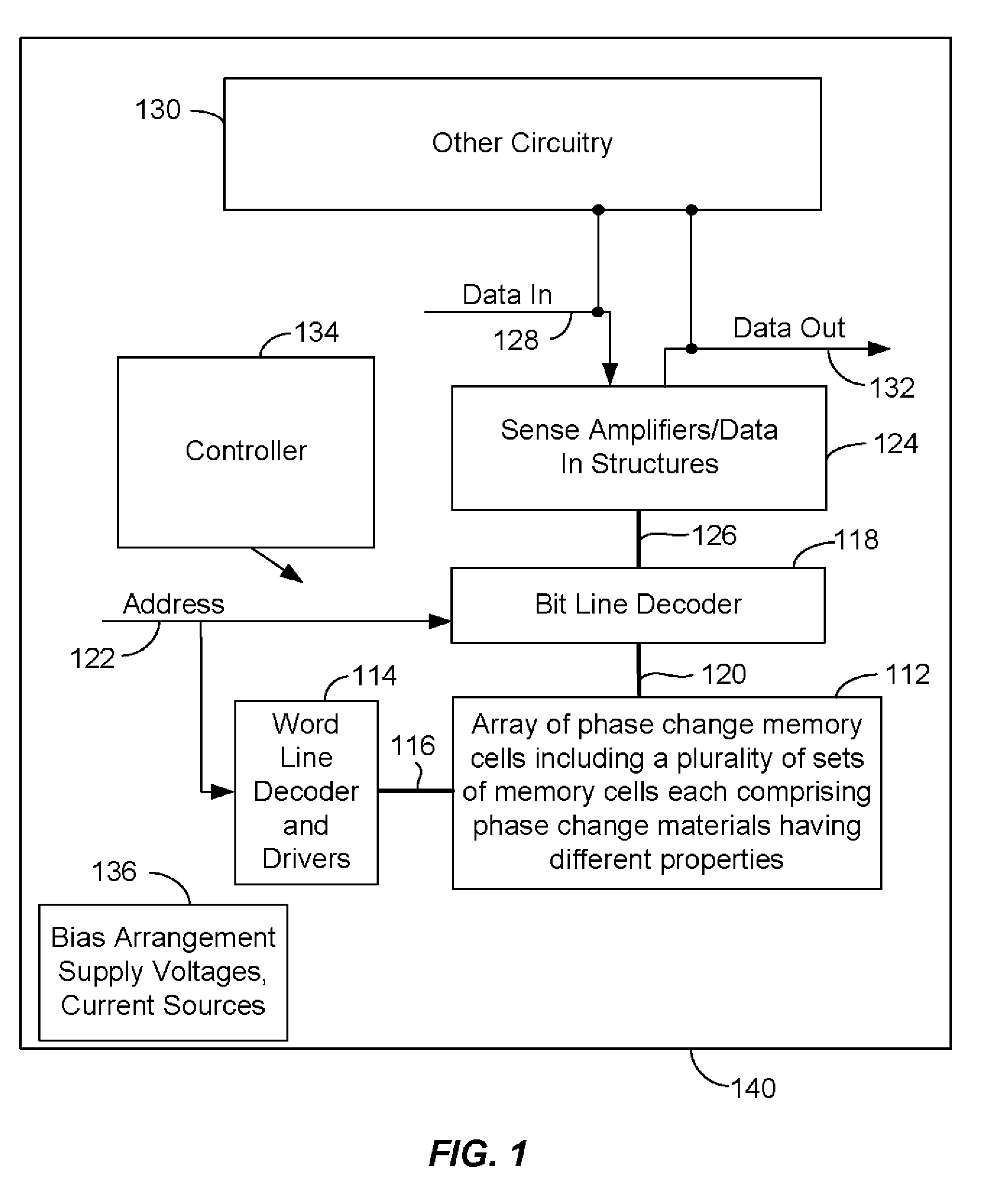
[0022]FIG. 1 is a block diagram of an integrated circuit 110 including a memory array 112 of phase change memory cells including a plurality of sets of memory cells comprising phase change materials having different properties. As described in more detail below, the phase change materials have different properties such that the sets of phase change memory cells have different operational memory characteristics.

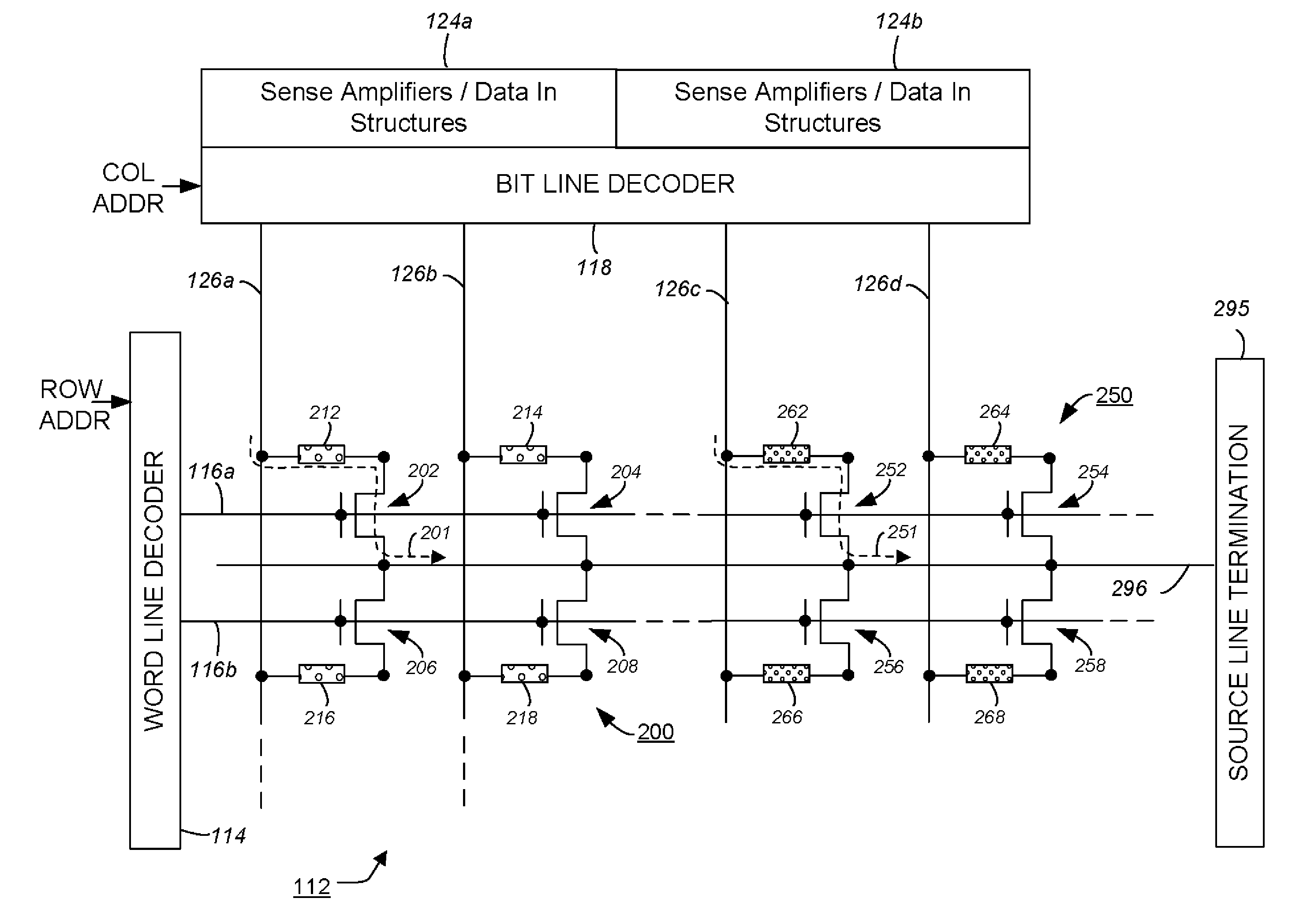
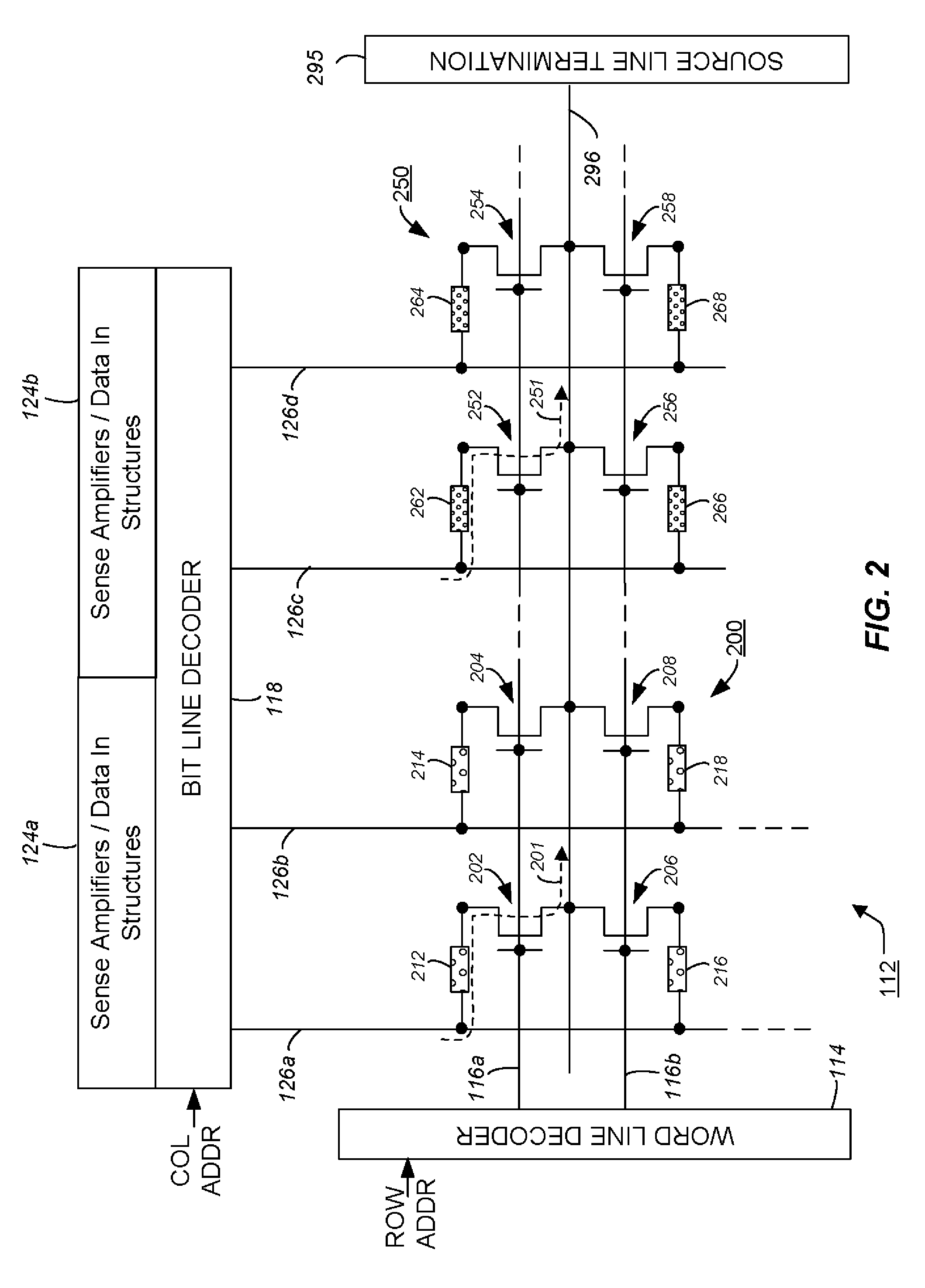
[0023]A word line decoder 114 having read, set and reset modes is coupled to and in electrical communication with a plurality of word lines 116 arranged along rows in the memory array 112. A bit line (column) decoder 118 is in electrical communication with a plurality of bit lines 120 arranged along columns in the array 112 for reading, setting, and resetting the phase change memory cells (not shown) in array 112. Addresses are supplied on bus 122 to word line decoder and drivers 114 and bit line decoder 118. Sense amplifiers and data-in structures in block 124, including volt...

second embodiment

[0064]FIG. 3 illustrates array 112 in which the first and second sets of memory cells 200, 250 comprise bipolar junction transistor access devices. Other alternative embodiments may include implementation of diode access devices. In some embodiments the first and second sets of memory cells 200, 250 comprise different types of access devices.

[0065]In some embodiments the plurality of sets of memory cells of array 112 may comprise memory elements having the same physical configuration. Alternatively, the plurality of sets of memory cells of array 112 may comprise various types of memory elements having different physical configurations. FIGS. 4A-4E illustrate cross-sectional views of various physical configurations for a memory element 400 which may implemented in the plurality of sets of memory cells of array 112. As will be understood, the present invention is not limited to the types of memory element physical configurations illustrated in FIGS. 4A-4E.

[0066]FIG. 4A is a simplified...


PUM


Abstract

Integrated circuits are described along with methods for manufacturing. An integrated circuit as described herein includes a plurality of memory cells on a substrate. The plurality of memory cells comprise a first set of memory cells comprising a first memory material, and a second set of memory cells comprising a second memory material. The first and second memory materials have different properties such that the first and second sets of memory cells have different operational memory characteristics.

Description

PARTIES TO A JOINT RESEARCH AGREEMENT[0001]International Business Machines Corporation, a New York corporation, and Macronix International Corporation, Ltd., a Taiwan corporation are parties to a Joint Research Agreement.BACKGROUND OF THE INVENTION[0002]1. Field of the Invention[0003]The present invention relates to memory devices based on phase change based memory materials, including chalcogenide based materials and other programmable resistance materials, and methods for manufacturing such devices.[0004]2. Description of Related Art[0005]In general, system-on-chip (SOC) technology is the integration of multiple subsystems of an electronic system within a single integrated circuit, and may contain digital, analog, mixed-signal, and radio-frequency functions. The various types of subsystems that may be integrated within the integrated circuit include microprocessor and microcontroller cores, digital signal processors (DSPs), configurable logic units, memory blocks, timing sources, ...

Claims


Application Information

Patent Timeline
Patent Type & Authority Applications(United States)
IPC IPC(8): G11C11/00H01L21/00
CPCG11C11/5678G11C13/0004H01L27/2436H01L27/2445H01L27/2463H01L45/04H01L45/1683H01L45/1233H01L45/143H01L45/144H01L45/146H01L45/148H01L45/1675H01L45/06H10B63/32H10B63/30H10B63/80H10N70/231H10N70/20H10N70/8825H10N70/884H10N70/826H10N70/8828H10N70/8833H10N70/066H10N70/063
Inventor LUNG, HSIANG-LAN
Owner MACRONIX INT CO LTD
Why Eureka
Try Eureka