Storage device using a multi-level flash memory as a single flash memory and method for the same

a storage device and multi-level technology, applied in the direction of memory adressing/allocation/relocation, digital storage, instruments, etc., can solve the problems of flash memory not being able to change data update-in-place, the price cost of slc nand flash memory is higher than that of slc nand flash memory, and the power consumption of nand mlc flash memory is more than that of slc mlc flash memory by 15%

Inactive Publication Date: 2010-02-25
GENESYS LOGIC INC
View PDF2 Cites 9 Cited by
  • Summary
  • Abstract
  • Description
  • Claims
  • Application Information

AI Technical Summary

Benefits of technology

[0011]It is therefore an object of the present invention to provide a storage device using a multi-level flash memory as a single flash memory to reduce cost of a storage device using a single flash memory.

Problems solved by technology

However, the flash memory may fail to change data update-in-place, in other words, erasing a block including the non-blank page is required prior to writing data into a non-blank page.
Additionally, power consumption of the NAND MLC flash memory is more than that of the SLC flash memory by 15%.
However, the price cost of SLC NAND flash memory is higher than that of MLC NAND flash memory.
For example, a 2 giga-bytes SLC flash memory is more expensive than that of a 4 giga-bytes MLC flash memory.

Method used


Image

  • Storage device using a multi-level flash memory as a single flash memory and method for the same
  • Storage device using a multi-level flash memory as a single flash memory and method for the same
  • Storage device using a multi-level flash memory as a single flash memory and method for the same

Examples


Embodiment Construction

[0024]Please refer to FIG. 4, which shows a block diagram of a storage device 10 and a host 5 according to a preferred embodiment of the present invention. The storage device 10 comprises a flash memory 20, a control interface 30, a write controller 40, and a read controller 50. The flash memory 20 is a multi-level cell (MLC) NAND flash memory having a plurality of pages 22 for storing data.

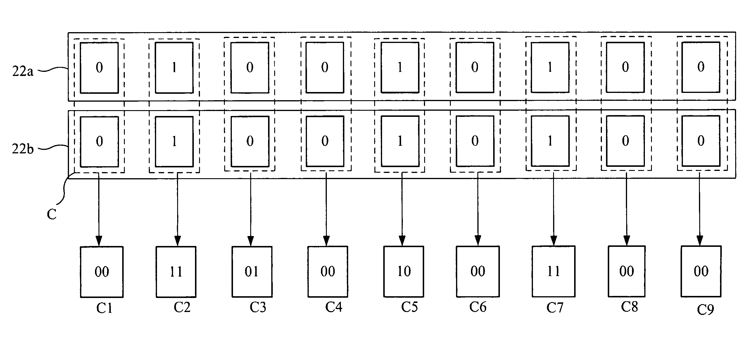
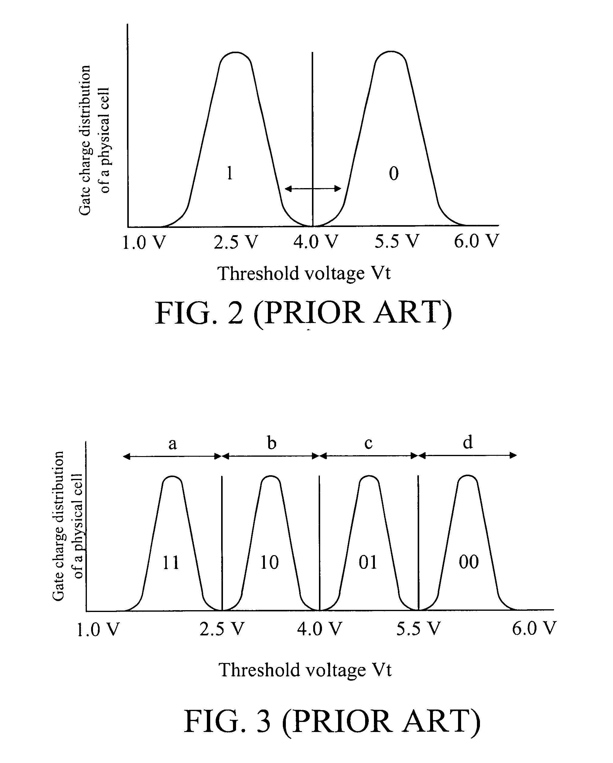
[0025]Please refer to FIGS. 4, 5 and 6. FIG. 5 is a flowchart of a method of using an MLC NAND flash memory as a single flash memory according to the present invention. FIG. 6 illustrates data access of pages of the flash memory shown in FIG. 4. The method comprises steps of:[0026]Step 500: Providing an MLC NAND flash memory having a plurality of physical cells. The physical cells form a first page and a second page. Each physical cell defines four threshold voltage ranges, each indicative of two-bit data.[0027]Step 502: upon receiving a first request to write first data into the first page, the ...


PUM


Abstract

A storage device includes a multi-level cell flash memory having a plurality of physical memory cells, a read controller, and a write controller. The physical memory cells form a first page and a second page. The write controller in response to a first request is used for writing first data into the first page, duplicating the first data as a second data and writing the second data into the second page. The read controller is used for adjusting the stored data value complying with a desired storing value. Each physical memory cell comprises four threshold voltage ranges indicative of two-bit logical values. The two-bit data is assigned as a first logical value accordingly in response to a two-bit data corresponding to a first and second threshold voltage ranges in a first physical memory cell. The two-bit data is assigned as a second logical value accordingly in response to a two-bit data corresponding to a third and fourth threshold voltage ranges in a second physical memory cell.

Description

BACKGROUND OF THE INVENTION[0001]1. Field of the Invention[0002]The present invention relates to a storage device using a flash memory and related method, and more particularly, to a storage device using a multi-level flash memory as a single flash memory and method for the same.[0003]2. Description of the Related Art[0004]A flash Memory, a non-volatile memory, may keep the previously stored written data upon shutdown. In contrast to other storage media, e.g. hard disks, soft disks, magnetic tapes and so on, the flash memory has advantages of small volume, light weight, vibration-proof, low power consumption, and no mechanical movement delay in data access, therefore, are widely used as storage media in consumer electronic devices, embedded systems, or portable computers.[0005]There are two kinds of flash memory: an NOR flash memory and an NAND flash memory. An NOR flash memory is characteristically of low driving voltage, fast access speed, high stability, and are widely applied in...

Claims


Application Information

Patent Timeline
Patent Type & Authority Applications(United States)
IPC IPC(8): G06F12/02G06F12/00
CPCG11C11/5628G11C2211/5641G11C16/0483G11C11/5642
Inventor CHEN, JU-PENG
Owner GENESYS LOGIC INC
Why Eureka
Try Eureka