Thin film transistor array substrate and method of fabricating the same

a technology of thin film transistors and array substrates, applied in the direction of transistors, electrical devices, semiconductor devices, etc., can solve the problems of difficult to achieve uniform electrical characteristics in a large display device, and achieve the effect of high charge mobility and uniform electrical characteristics

Active Publication Date: 2010-03-04
SAMSUNG DISPLAY CO LTD
View PDF1 Cites 51 Cited by
  • Summary
  • Abstract
  • Description
  • Claims
  • Application Information

AI Technical Summary

Benefits of technology

[0009]Aspects of the present invention include a thin film transistor array substrate which has a high charge mobility and allows uniform electrical characteristics to be achieved when applied to a large display device.

Problems solved by technology

Polycrystalline silicon thin film transistors, on the other hand, have a high charge mobility of approximately several hundred cm2 / Vs, but make it difficult to achieve uniform electrical characteristics in a large display device.

Method used


Image

  • Thin film transistor array substrate and method of fabricating the same
  • Thin film transistor array substrate and method of fabricating the same
  • Thin film transistor array substrate and method of fabricating the same

Examples


Embodiment Construction

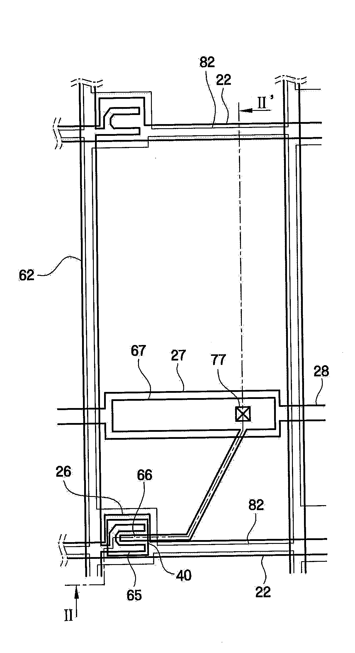
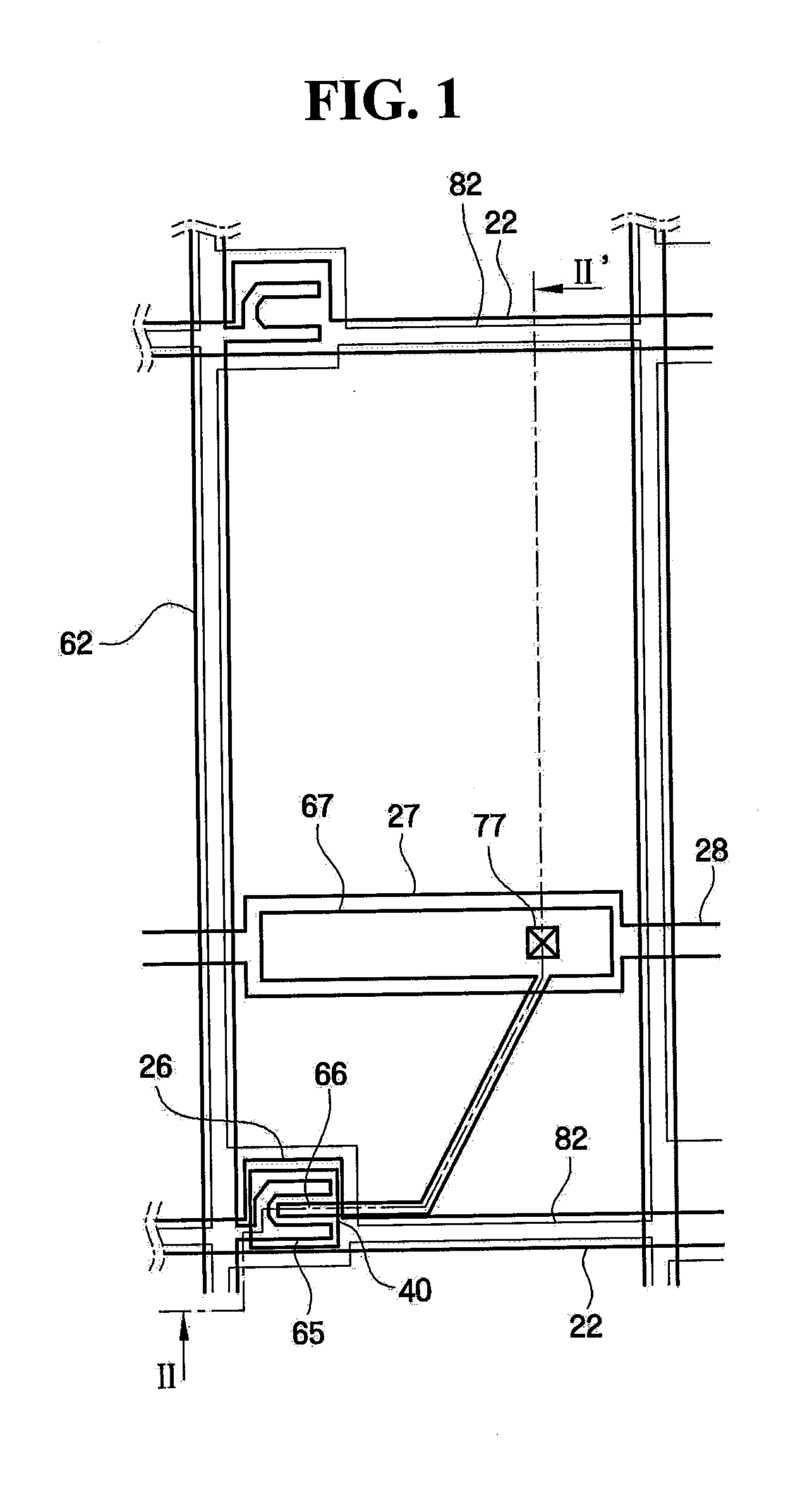
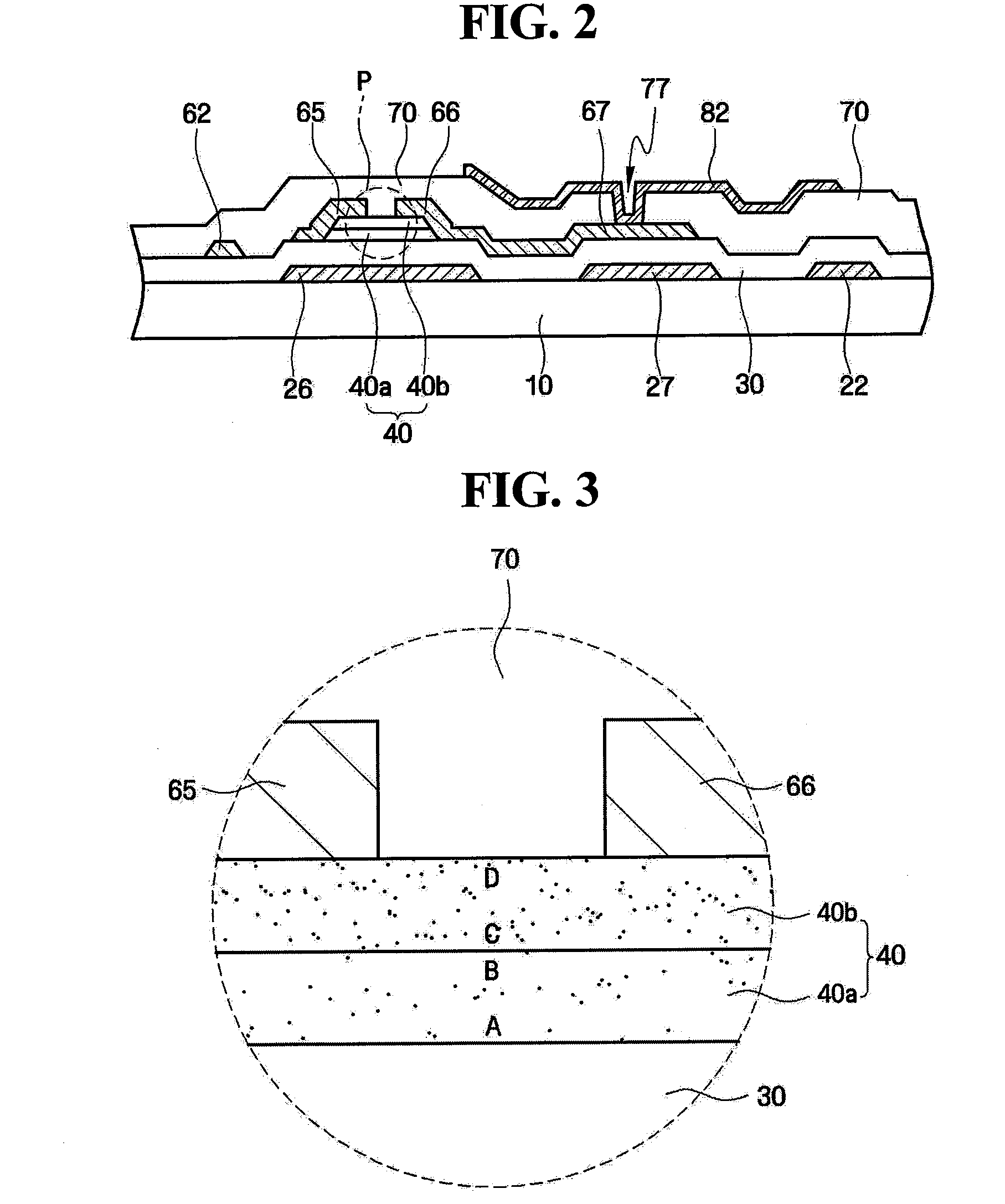
[0025]The invention will now be described more fully hereinafter with reference to the accompanying drawings, in which exemplary embodiments of the present invention are illustrated. The invention may, however, be embodied in different forms and should not be construed as limited to the embodiments set forth herein. Rather, these embodiments are provided so that this disclosure will be thorough and complete, and will fully convey the scope of the present invention to those skilled in the art.

[0026]It will be understood that when an element is referred to as being “connected” or “coupled” to another element, it can be directly connected or coupled to the other element or intervening elements may be present. In contrast, when an element is referred to as being “directly connected” or “directly coupled” to another element, there are no intervening elements present. Like numbers denote like elements throughout the specification. As used herein the term “and / or” includes any and all comb...


PUM


Abstract

A thin film transistor array substrate having a high charge mobility and that can raise a threshold voltage, and a method of fabricating the thin film transistor array substrate are provided. The thin film transistor array substrate includes: an insulating substrate; a gate electrode formed on the insulating substrate; an oxide semiconductor layer comprising a lower oxide layer formed on the gate electrode and an upper oxide layer formed on the lower oxide layer, such that the oxygen concentration of the upper oxide layer is higher than the oxygen concentration of the lower oxide layer; and a source electrode and a drain electrode formed on the oxide semiconductor layer and separated from each other.

Description

CROSS-REFERENCE TO RELATED APPLICATION[0001]This application claims priority from Korean Patent Application No. 10-2008-0086277 filed on Sep. 2, 2008 in the Korean Intellectual Property Office, the disclosure of which is incorporated herein by reference in its entirety.BACKGROUND OF THE INVENTION[0002]1. Field of the Invention[0003]The present invention relates to a thin film transistor array substrate and a method of fabricating the same, and more particularly, to a thin film transistor array substrate and a method of fabricating the same, in which electrical characteristics of an oxide semiconductor layer are improved.[0004]2. Description of the Related Art[0005]A liquid crystal display (LCD) is one of most widely used flat panel display configurations. The LCD includes two substrates on which electrodes are formed, and a liquid crystal layer interposed between the two substrates. Voltages are applied to the electrodes to realign the liquid crystal molecules of the liquid crystal ...

Claims


Application Information

Patent Timeline
Patent Type & Authority Applications(United States)
IPC IPC(8): H01L29/786H01L21/336
CPCH01L29/7869H01L27/1225H01L29/06
Inventor KIM, DO-HYUNLEE, JE-HUNYUN, PIL-SANGLEE, DONG-HOONKIM, BONG-KYUN
Owner SAMSUNG DISPLAY CO LTD
Why Eureka
Try Eureka