Wafer carrier with varying thermal resistance

a technology of thermal resistance and carrier, applied in the direction of liquid surface applicators, coatings, chemical vapor deposition coatings, etc., can solve the problems of non-uniform heat transfer, and achieve the effect of improving temperature uniformity and minimizing conta

Inactive Publication Date: 2010-03-04
VEECO INSTR
View PDF39 Cites 297 Cited by
  • Summary
  • Abstract
  • Description
  • Claims
  • Application Information

AI Technical Summary

Benefits of technology

[0011]Yet another aspect of the invention provides a wafer carrier. A wafer carrier according to this aspect of the invention desirably includes a body having oppositely-facing top and bottom surfaces and a central axis extending between the top and bottom surfaces. The top surface of the body typically has a plurality of pockets, each such pocket having a peripheral wall. The peripheral wall of each pocket most preferably has a plurality of spaced-apart projections in a region of the peripheral wall remote from the central axis of the wafer carrier, the projections being adapted to engage spaced-apart portions of an edge of a wafer disposed in the pocket. As further explained below, such projections help to minimize contact between the edge of the wafer and the peripheral wall, and help to hold the wafer centered in the pocket. These effects in turn tend to promote better temperature uniformity across the top surface of each wafer.

Problems solved by technology

The bowing causes non-uniformity in heat transfer from the wafer carrier to the wafer within each wafer.

Method used


Image

  • Wafer carrier with varying thermal resistance
  • Wafer carrier with varying thermal resistance
  • Wafer carrier with varying thermal resistance

Examples


Embodiment Construction

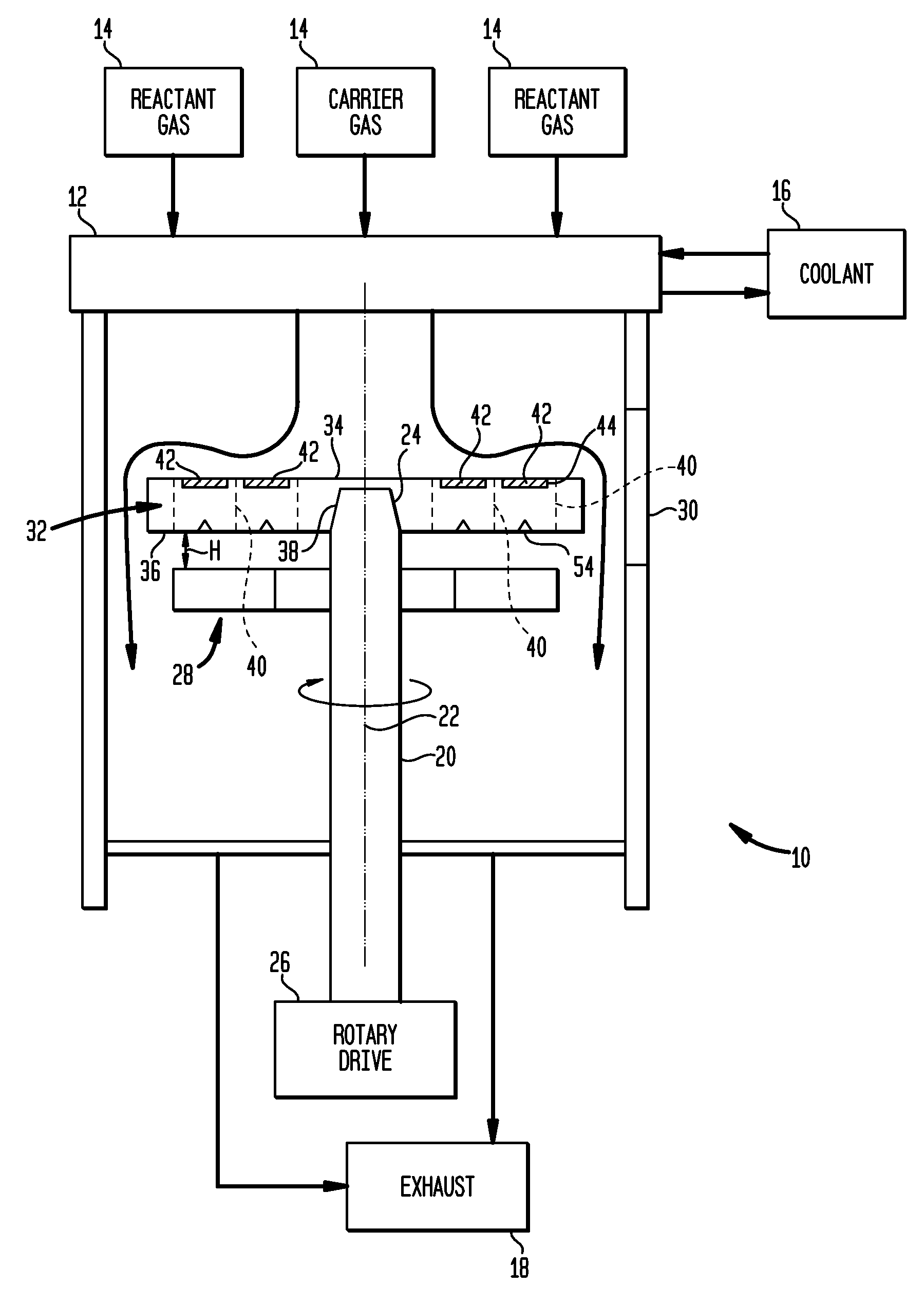
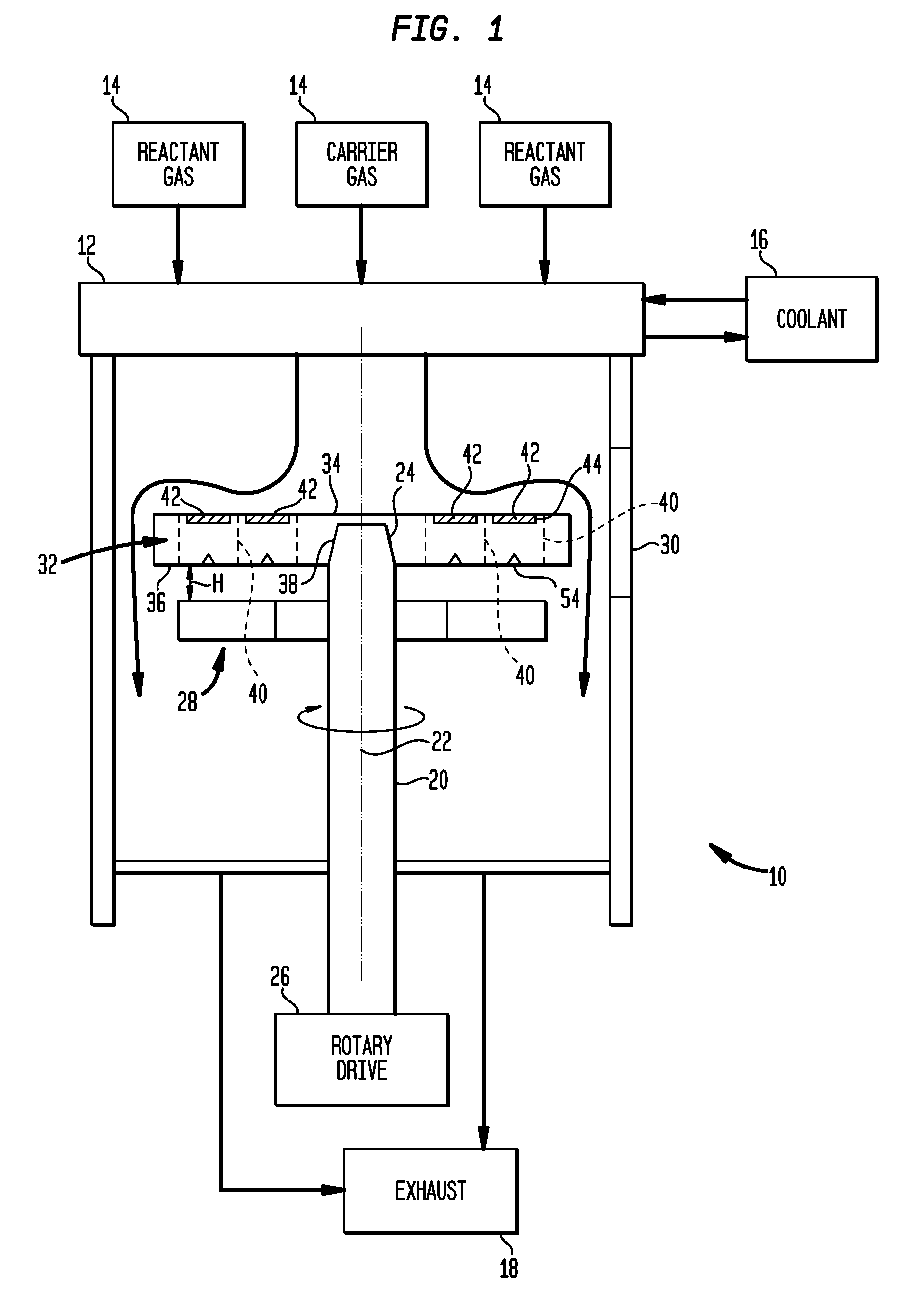
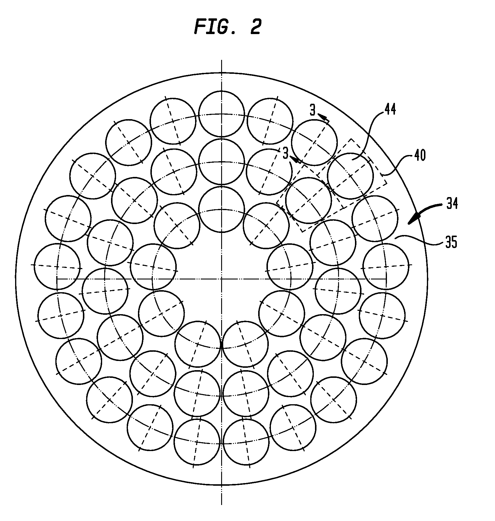
[0023]Chemical vapor deposition apparatus in accordance with one embodiment of the invention includes a reaction chamber 10 having a gas distribution element 12 arranged at one end of the chamber. The end having the gas distribution element 12 is referred to herein as the “top” end of the chamber 10. This end of the chamber typically, but not necessarily, is disposed at the top of the chamber in the normal gravitational frame of reference. Thus, the downward direction as used herein refers to the direction away from the gas distribution element 12; whereas the upward direction refers to the direction within the chamber, toward the gas distribution element 12, regardless of whether these directions are aligned with the gravitational upward and downward directions. Similarly, the “top” and “bottom” surfaces of elements are described herein with reference to the frame of reference of chamber 10 and element 12. Gas distribution element 12 is connected to sources 14 of gases to be used i...


PUM

PropertyMeasurementUnit
temperatureaaaaaaaaaa
thicknessaaaaaaaaaa
diameteraaaaaaaaaa

Abstract

In chemical vapor deposition apparatus, a water carrier (32) has a top surface (34) holding the wafers and a bottom surface (36) heated by radiant heat transfer from a heating element (28). The bottom surface (36) of the wafer carrier is non-planar due to features such as depressions (54) so that the wafer carrier has different thickness at different locations. The thicker portions of the wafer carrier have higher thermal resistance. Differences in thermal resistance at different locations counteract undesired non-uniformities in heat transfer to the wafer. The wafer carrier may have pockets with projections (553, 853) for engaging spaced-apart locations on the edges of the wafer.

Description

CROSS-REFERENCE TO RELATED APPLICATIONS[0001]The present application claims the benefit of the filing date of U.S. Provisional Patent Application No. 61 / 190,494, filed Aug. 29, 2008, the disclosure of which is hereby incorporated by reference herein.BACKGROUND OF THE INVENTION[0002]The present invention relates to wafer processing apparatus, to wafer carriers for use in such processing apparatus, and to methods of wafer processing.[0003]Many semiconductor devices are formed by epitaxial growth of a semiconductor material on a substrate. The substrate typically is a crystalline material in the form of a disc, commonly referred to as a “wafer.” For example, devices formed from compound semiconductors such as III-V semiconductors typically are formed by growing successive layers of the compound semiconductor using metal organic chemical vapor deposition or “IMOCVD.” In this process, the wafers are exposed to a combination of gases, typically including a metal organic compound and a sou...

Claims


Application Information

Patent Timeline
Patent Type & Authority Applications(United States)
IPC IPC(8): C23C16/46C23C16/00
CPCC23C16/4584C23C16/4583H01L21/68735H01L21/68764H01L21/67103H01L21/68771C23C16/46H01L21/205H01L21/673H01L21/683
Inventor VOLF, BORISSODERMAN, BREIDARMOUR, ERIC A.
Owner VEECO INSTR
Why Eureka
Try Eureka