Semiconductor light emitting device

a technology of light-emitting devices and semiconductors, which is applied in the direction of semiconductor devices, basic electric elements, electrical appliances, etc., can solve the problems of reducing the light reflection efficiency of reflectors, and achieve the effect of increasing brightness

Active Publication Date: 2010-03-25
ROHM CO LTD
View PDF10 Cites 14 Cited by
  • Summary
  • Abstract
  • Description
  • Claims
  • Application Information

AI Technical Summary

Benefits of technology

[0005]The present invention has been proposed under the circumstances described above. It is, therefore, an object

Problems solved by technology

However, such a shape and size may lead to a reduction i

Method used


Image

  • Semiconductor light emitting device
  • Semiconductor light emitting device
  • Semiconductor light emitting device

Examples


Embodiment Construction

[0028]Preferred embodiments of the present invention will be described below with reference to the accompanying drawings.

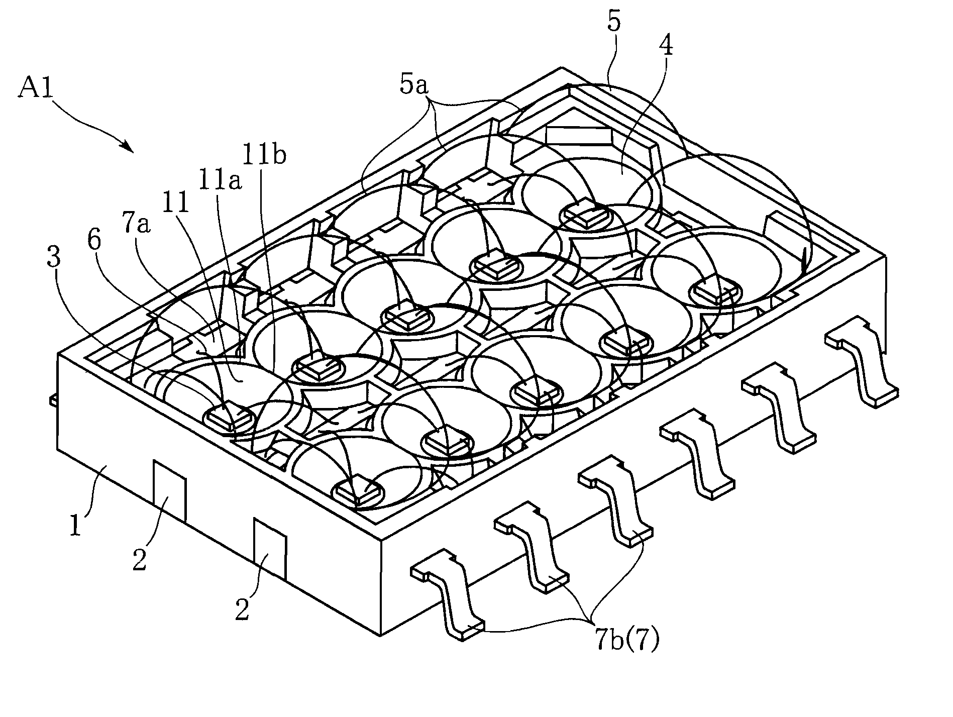
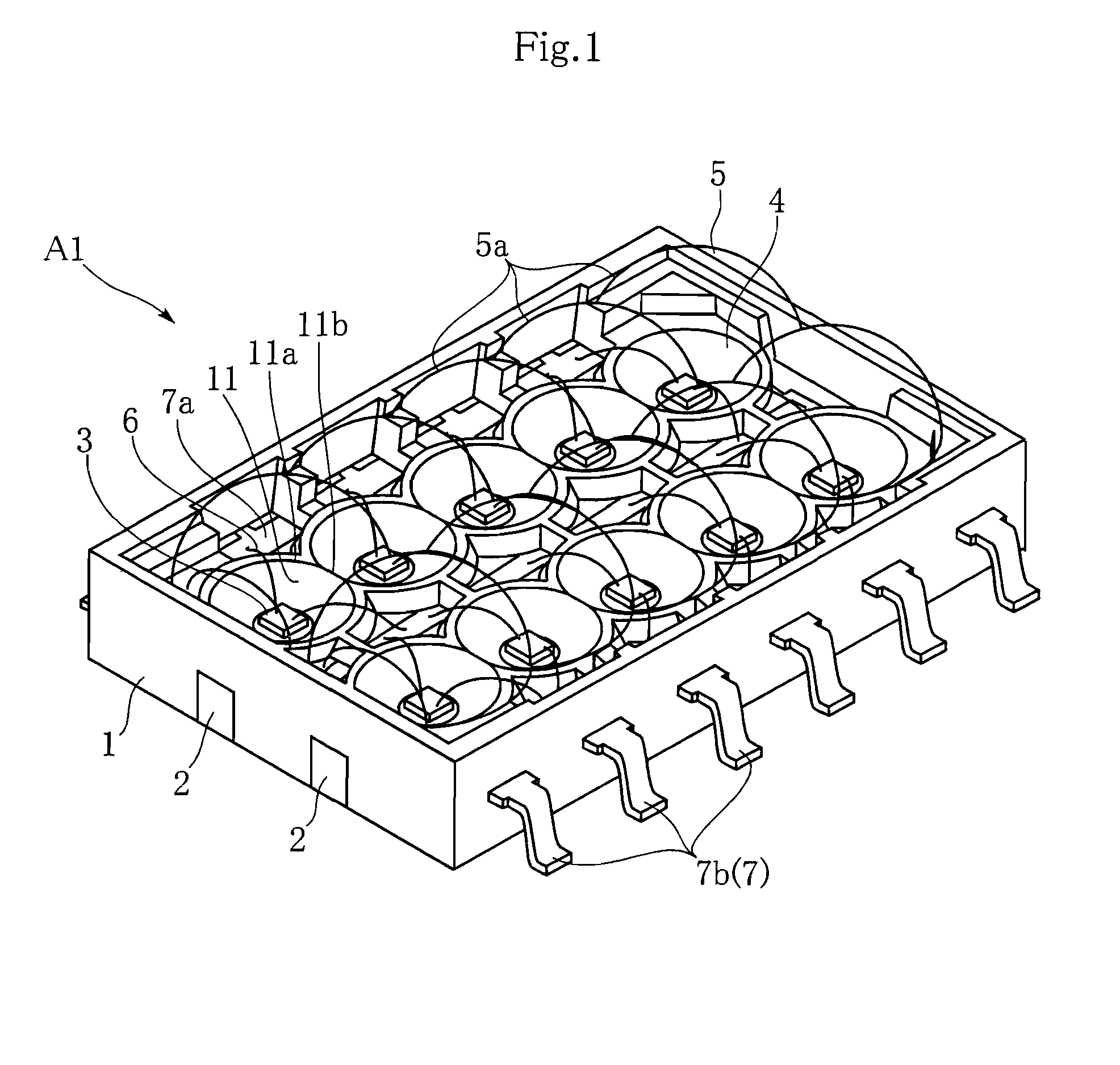
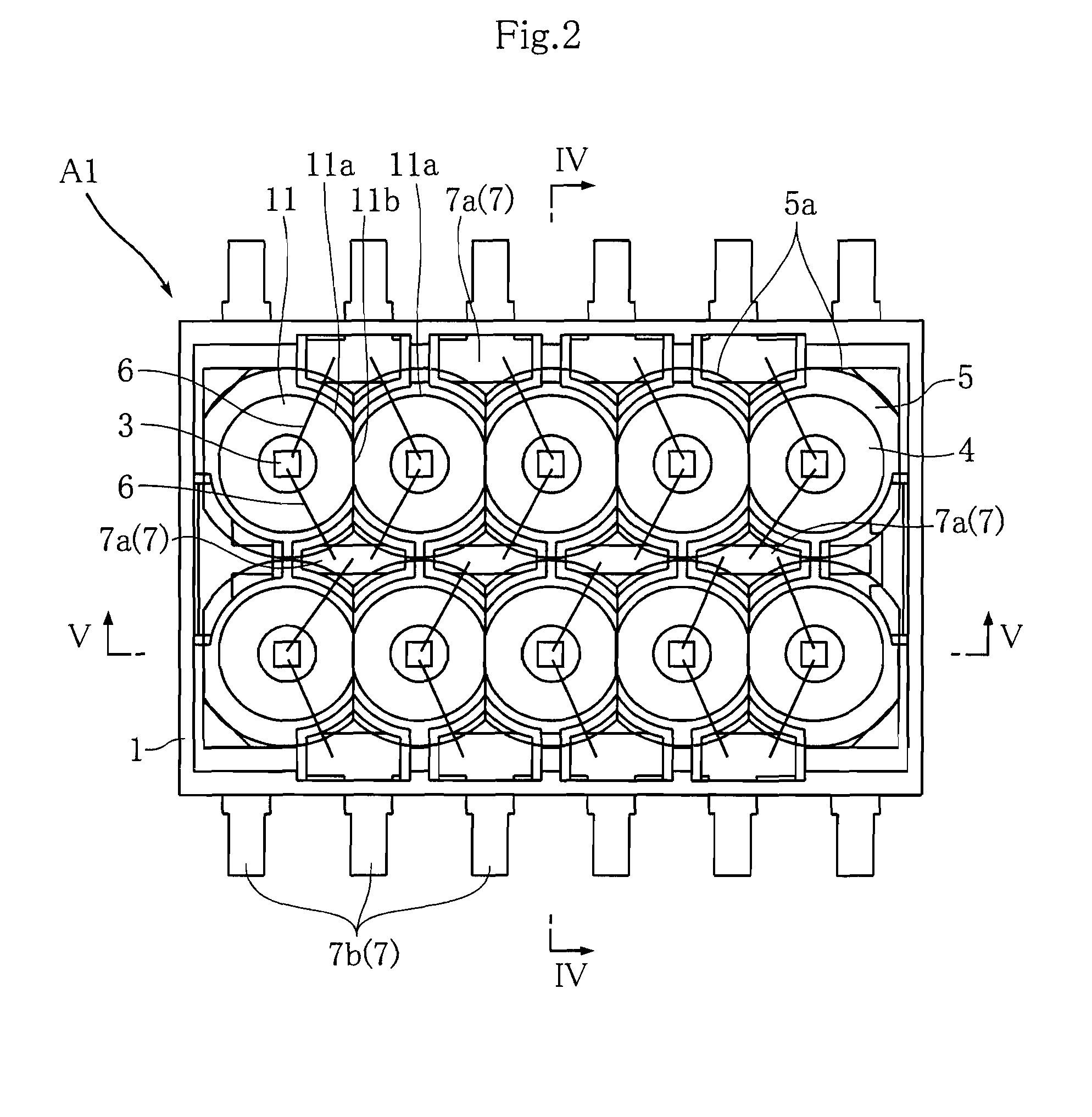
[0029]FIGS. 1-6 show a semiconductor light emitting device according to a first embodiment of the present invention. The illustrated semiconductor light emitting device A1 includes a case 1, two heat dissipaters 2, a plurality of LED chips 3, fluorescent resin 4, transparent resin 5, a plurality of wires 6 and a plurality of leads 7. The semiconductor light emitting device A1 functions as a surface-emitting light source device by turning on the plurality of LED chips 3 simultaneously. In FIGS. 4-6, the illustration of the wires 6 is omitted. In FIG. 6, the illustration of the fluorescent resin 4 and the transparent resin 5 is also omitted.

[0030]The case 1 is generally in the form of a thin rectangular parallelepiped and made of e.g. white resin. The case 1 is used as the base of the semiconductor light emitting device A1. The case 1 is formed with a plurality of r...


PUM


Abstract

A semiconductor light emitting device (A1) includes a case (1) and a plurality of semiconductor light emitting elements (3) arranged in the case. The case (1) is formed with a plurality of reflectors (11) each in the form of a truncated cone surrounding a respective one of the semiconductor light emitting elements (3). Current is applied to each of the semiconductor light emitting elements (3) via two wires (6). Each of the wires (6) includes a first end, and a second end opposite to the first end. The first end is connected to the semiconductor light emitting element (3), whereas the second end is located outside the space surrounded by the reflector (11).

Description

TECHNICAL FIELD[0001]The present invention relates to a semiconductor light emitting device including a plurality of semiconductor light emitting elements.BACKGROUND ART[0002]FIG. 15 shows an example of conventional semiconductor light emitting device (see e.g. Patent Document 1 identified below). The semiconductor light emitting device X shown in the figure includes a printed wiring board 91, a plurality of LED chips 92, a plurality of wires 93, a plurality of fluorescent resin members 94 and a transparent resin member 95. The LED chips 92 are mounted in a matrix on the printed wiring board 91. Each of the LED chips 92 is electrically connected to the wiring pattern (not shown) of the printed wiring board 91 via two wires 93. The printed wiring board 91 is formed with a plurality of reflectors 91a. Each of the reflectors 91a surrounds a respective one of the LED chips 92 and the two wires 93. The surfaces of the reflectors have a high reflectivity. The fluorescent resin members 94 ...

Claims


Application Information

Patent Timeline
IPC IPC(8): H01L33/00H01L33/60H01L33/62
CPCH01L25/0753H01L33/60H01L33/62H01L2224/48091H01L2224/48247H01L2924/01079H01L2924/01004H01L2924/00014
Inventor KOBAYAKAWA, MASAHIKO
Owner ROHM CO LTD
Why Eureka
Try Eureka