Substrate bonded MEMS sensor

a technology of mems sensor and glass substrate, applied in the field of mems sensor, can solve the problems of difficult to define the opposing distance of glass substrate with high precision, difficult to provide an appropriate movable clearance (margin) between the movable electrode portion and the glass substrate, and difficult to form a sealing layer with a fine pattern

Inactive Publication Date: 2010-03-25
ALPS ALPINE CO LTD
View PDF19 Cites 44 Cited by
  • Summary
  • Abstract
  • Description
  • Claims
  • Application Information

AI Technical Summary

Problems solved by technology

Moreover, since the opposing distance of the upper and lower glass substrates is determined by the thickness of the glass frit seal that hermetically seals the circumference of the movable region of the movable electrode portion, it is difficult to define the opposing distance of the glass substrates with high precision.
As a result, it is difficult to provide an appropriate movable clearance (margin) between the movable electrode portion and the glass substrates, necessary for the operation of the movable electrodes.
Moreover, since the glass frit seal is melted down and solidified to form a sealing layer, it is difficult to form a sealing layer with a fine pattern.
Therefore, the overall size of the package becomes too large.
Therefore, it is necessary to ensure a marginal dimension between these electrode layers or lead layers and the movable electrode layer, which makes it difficult to realize a low profile of the package.

Method used


Image

  • Substrate bonded MEMS sensor
  • Substrate bonded MEMS sensor
  • Substrate bonded MEMS sensor

Examples


first embodiment

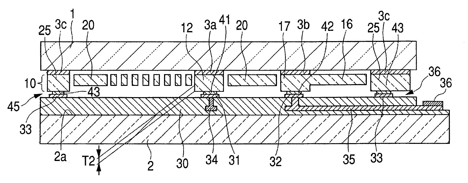
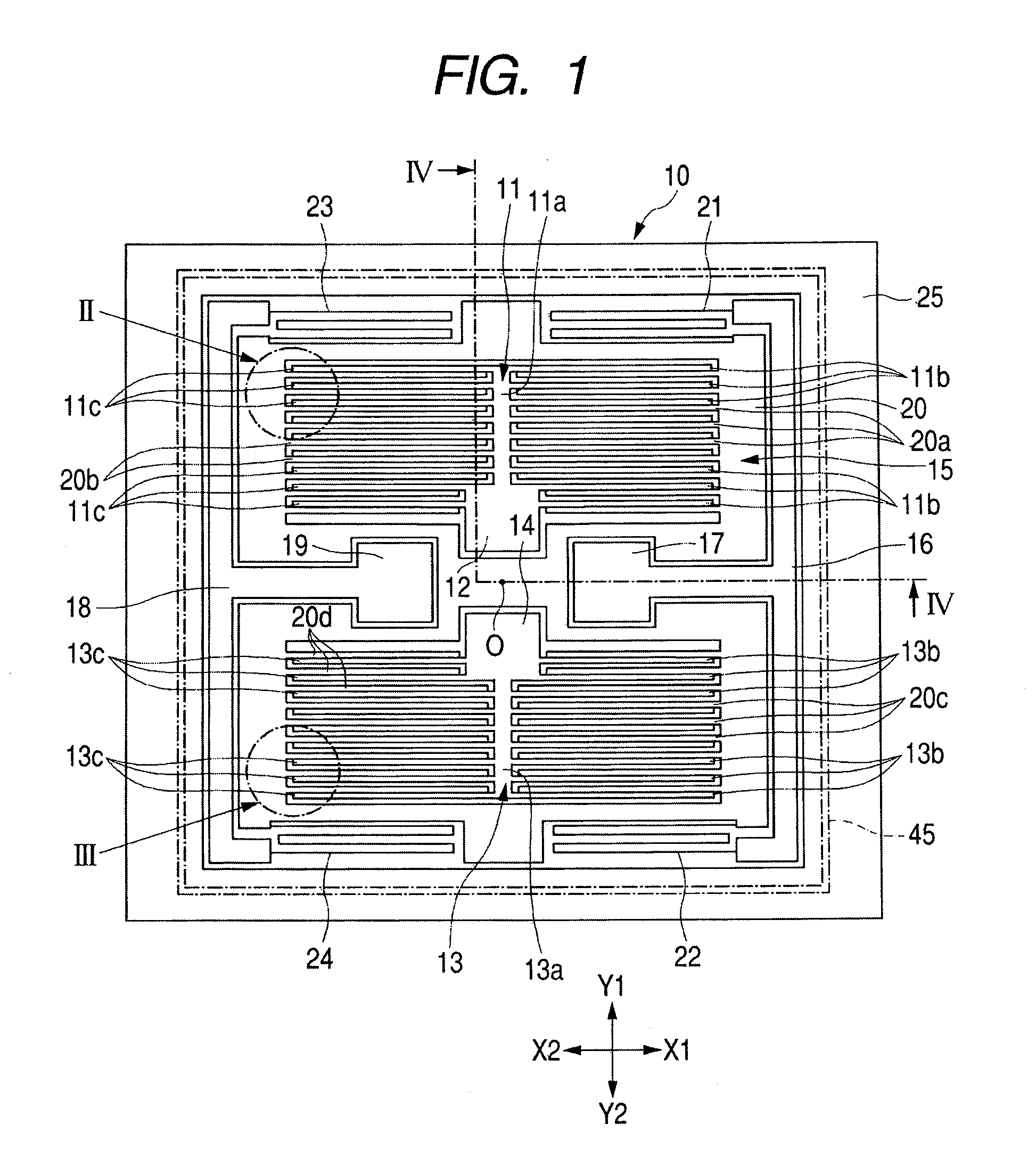
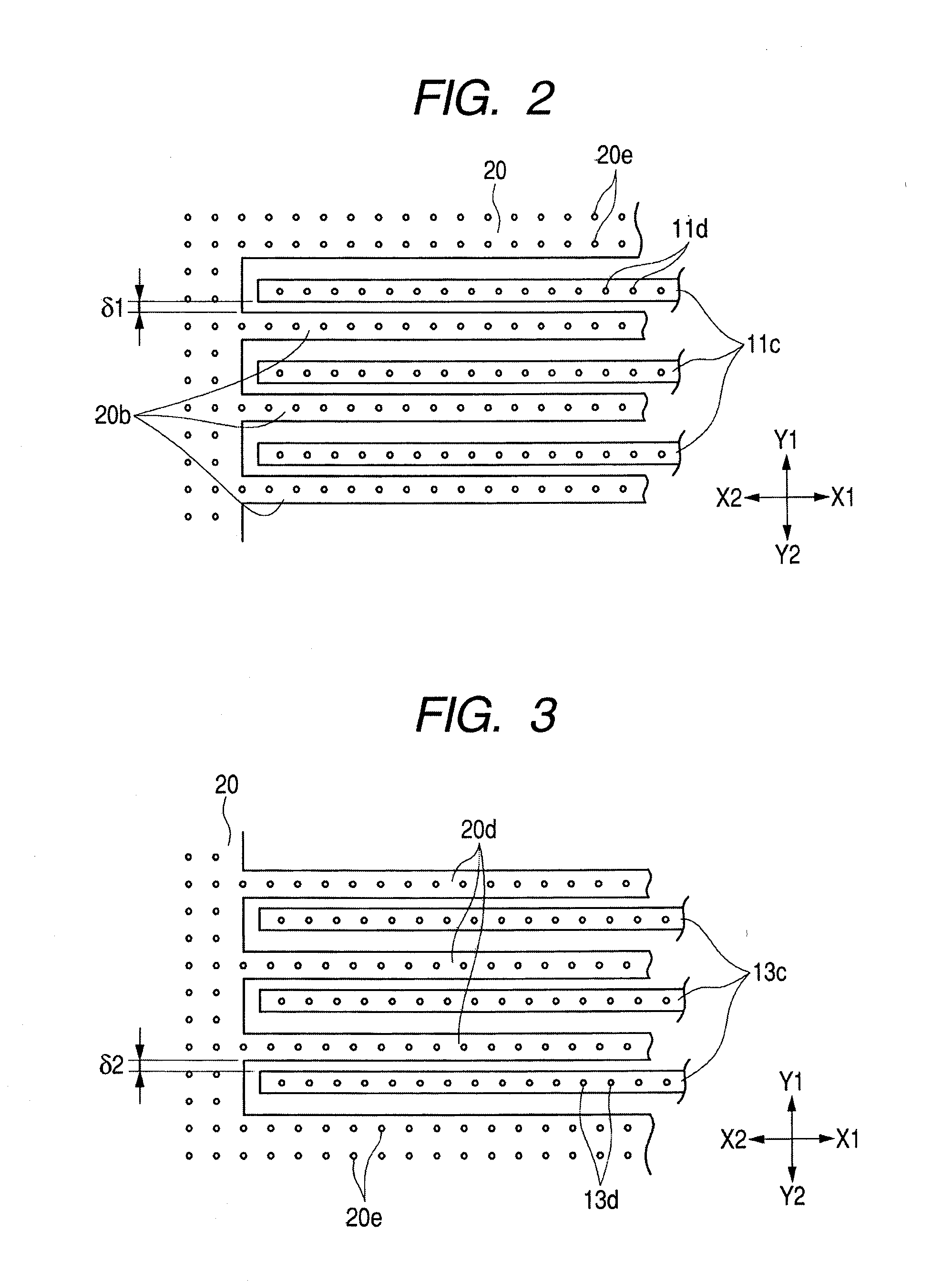
[0032]FIG. 1 is a top plan view of a MEMS sensor according to the first embodiment of the invention, illustrating movable electrode portion, a fixed electrode portion, and a frame layer. In FIG. 1, the illustrations of a first substrate and a second substrate are omitted. FIG. 2 is an enlarged view of the II portion in FIG. 1, and FIG. 3 is an enlarged view of the III portion in FIG. 1. FIG. 4 is a cross-sectional view illustrating the overall structure of the MEMS sensor, taken along the IV-IV lines in FIG. 1. FIG. 5 is a cross-sectional view for describing the method for fabricating the MEMS sensor. In FIGS. 4 and 5, the arrangements of respective layers are reversed upside down.

[0033]As illustrated in FIG. 4, the MEMS sensor has such a configuration that a functional layer 10 is sandwiched between a first substrate 1 and a second substrate 2. The respective portions of the functional layer 10 and the first substrate 1 are bonded together via a first insulating layer 3a, 3b, or 3c...

second embodiment

[0075]FIGS. 6A and 6B are cross-sectional views of a MEMS sensor according to the second embodiment of the invention, illustrating the VI portion in FIG. 4 in the enlarged views.

[0076]In the embodiment illustrated in FIG. 6A, on the surface of the conductive supporting portion 17 of the movable electrode portion 15, a groove 51 is formed so as to surround the bonding portion in which the metallic connection layer 42 and the connection electrode portion 32 are bonded together by eutectic bonding or diffusion bonding. The groove 51 may be continuously formed so as to surround the entire circumference of the bonding portion or may be discontinuously formed at intervals so as to surround the bonding portion.

[0077]In the embodiment illustrated in FIG. 6B, on the surface of the conductive supporting portion 17 of the movable electrode portion 15, a groove 52 is formed so as to surround the bonding portion of the metallic connection layer 42 and the connection electrode portion 32. The gro...

third embodiment

[0080]FIG. 7 is a cross-sectional view illustrating the MEMS sensor according to the third embodiment of the invention.

[0081]The MEMS sensor uses an IC package 100 instead of the second substrate 2. The IC package 100 incorporates therein a detection circuit, or the like, capable of detecting a change in the electrostatic capacitance between the counter electrodes and the movable counter electrodes.

[0082]The second insulating layer 30 is formed on an upper surface 101 of the IC package 100, and the connection electrode portions 31 and 32 and the sealing electrode portion 33 are formed on the surface of the second insulating layer 30. The connection electrode portions 31 and 32 are electrically connected to electrode pads that appear on the upper surface 101 of the IC package 100 via connection layers 134 and 135 such as through-holes configured to penetrate through the second insulating layer 30 and are connected to an electric circuit incorporated into the IC package 100.

[0083]In t...


PUM


Abstract

A MEMS sensor includes a first substrate; a second substrate; a movable electrode portion and a fixed electrode portion which are arranged between the first substrate and the second substrate, wherein: conductive supporting portions of the movable electrode portion and the fixed electrode portion are, respectively, fixedly secured to a surface of the first substrate via a first insulating layer; a second insulating layer, a lead layer buried into the second insulating layer, and connection electrode portions that are electrically connected to the lead layer to be individually connected to the conductive supporting portions are provided on a surface of the second substrate; a metallic connection layer is formed on the surface of one of the respective conductive supporting portions; one of the respective connection electrode portions and the metallic connection layer are bonded together by eutectic bonding or diffusion bonding; and, at least each of the connection electrode portions has a thickness of about 4 μm or smaller.

Description

CROSS REFERENCE TO RELATED APPLICATION[0001]The present invention contains subject matter related to and claims priority to Japanese Patent Applications JP 2008-242020, JP 2008-242025, and JP 2008-242026 filed in the Japanese Patent Office on Sep. 22, 2008, the entire contents of which being incorporated herein by reference.BACKGROUND[0002]1. Technical Field[0003]The present invention relates to MEMS (Micro-Electro-Mechanical Systems) sensors which are formed by microfabricating a silicon layer, and more particularly, to an MEMS sensor which has a low profile and exhibits an excellent ability to hermetically seal a movable region.[0004]2. Related Art[0005]MEMS sensors are formed with a movable electrode portion and a fixed electrode portion by microfabricating a silicon (Si) wafer that constitutes an SOI (Silicon on Insulator) layer. The micro sensors can be used as acceleration sensors, pressure sensors, vibrating gyro-sensors, or micro relays, depending on the operation of the mov...

Claims


Application Information

Patent Timeline
Patent Type & Authority Applications(United States)
IPC IPC(8): H01L29/84
CPCB81B2207/097B81B7/007
Inventor SATO, KIYOSHIKOBAYASHI, KIYOSHIUTO, YOSHITAKAKIKUIRI, KATSUYATAKAHASHI, KAZUYOSHISUZUKI, JUNGOCHOU, HIDEKITAKAHASHI, TORUOHKAWA, HISANOBU
Owner ALPS ALPINE CO LTD
Why Eureka
Try Eureka