

Method of forming wiring board and wiring board obtained
a technology of wiring board and conductive pattern, which is applied in the direction of conductive pattern formation, non-metallic protective coating application, dielectric characteristics, etc., can solve the problems of limiting the type of substrate, affecting the efficiency of the treatment process, and increasing the running cost and the size of the apparatus for performing treatment at high temperature. , to achieve the effect of preventing migration and high reliability
- Summary
- Abstract
- Description
- Claims
- Application Information
AI Technical Summary
Benefits of technology
Problems solved by technology
Method used
Image

Examples
first embodiment
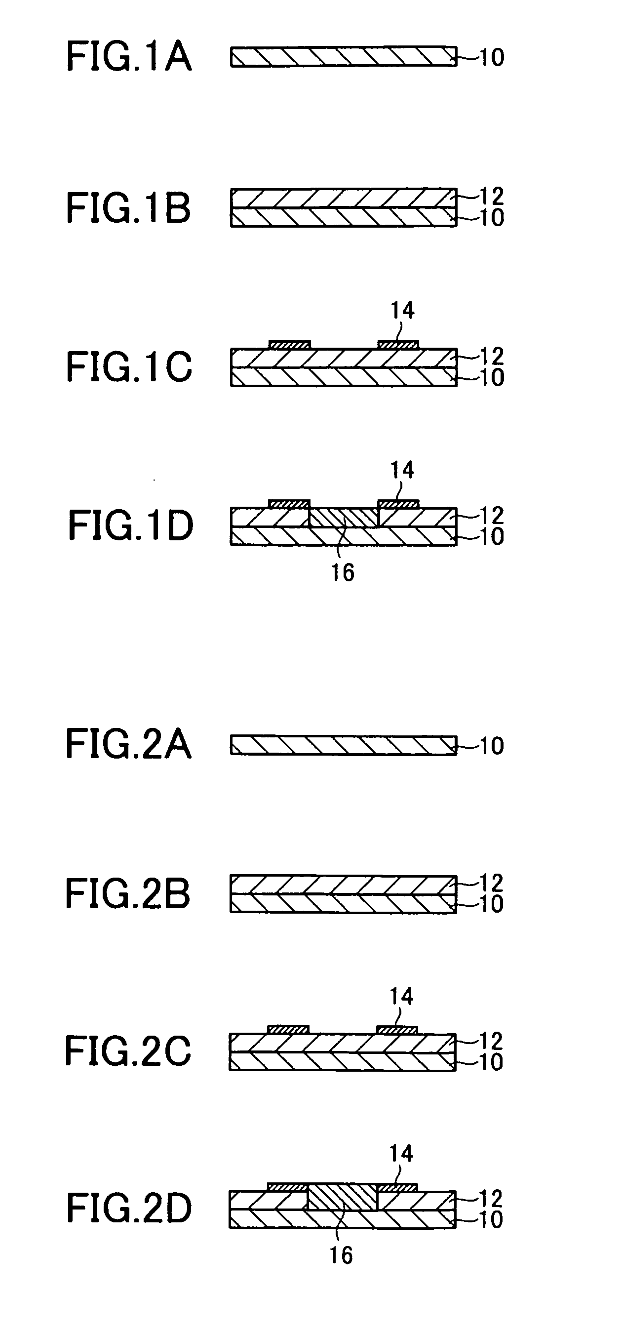
[0045]The wiring board forming method according to the first embodiment is described below with reference to FIGS. 1A to 1D.
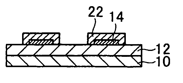
[0046]A receptive layer 12 of a porous structure is formed on a surface of a substrate 10 as shown in FIG. 1A to prepare a receptive layer-bearing substrate as shown in FIG. 1B. The receptive layer 12 may be formed on the whole surface of the substrate 10 but is preferably formed only at portions where a conductive pattern (wiring) is to be formed, by ejecting and applying a functional liquid containing a receptive layer material by an ink-jet system in order to prevent migration from occurring.
[0047]Then, as shown in FIG. 1C, patterned conductive metallic portions (conductive pattern) 14 are formed on the receptive layer 12. The conductive metallic portions 14 are formed by ejecting a colloidal metal solution for drawing by the ink-jet system based on image data of a conductive pattern.
[0048]A thermal ink-jet system or a piezoelectric ink-jet system may be use...
second embodiment
[0061]The wiring board forming method according to the second embodiment is described below with reference to FIGS. 2A to 2D.
[0062]In order to simplify the description, different portions from those of the first embodiment are only described in detail. Like elements are denoted by the same reference symbols and formed by the same method. The same treatments are also not described in detail.
[0063]A receptive layer 12 of a porous structure is formed on a surface of a substrate 10 as shown in FIG. 2A to prepare a receptive layer-bearing substrate as shown in FIG. 2B.
[0064]Then, as shown in FIG. 2C, a colloidal metal solution is applied to the receptive layer 12 by the ink-jet system to form patterned conductive metallic portions 14.
[0065]Then, an insulating resin in the form of a migration-proof solution is applied onto the receptive layer 12 exposed between mutually adjacent conductive metallic portions 14 and cured to form an insulating resin portion 16 in the space between the mutua...
third embodiment
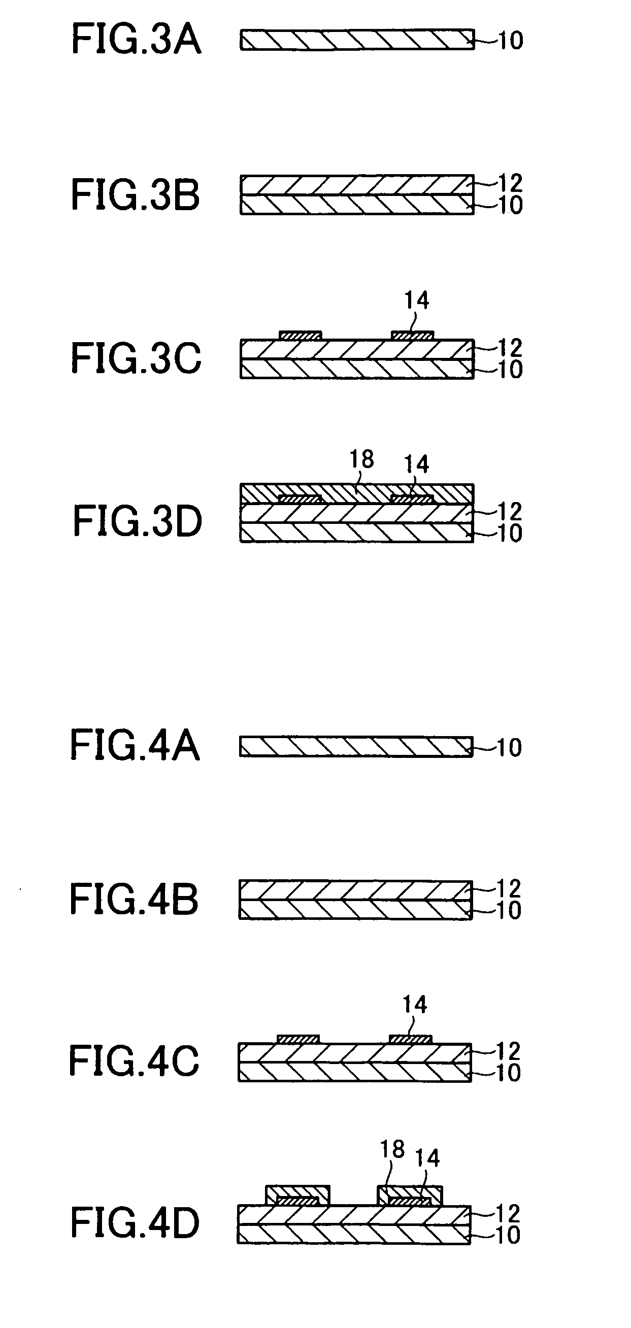
[0067]The wiring board forming method according to the third embodiment is described below with reference to FIGS. 3A to 3D.
[0068]In order to simplify the description, different portions from those of the first and second embodiments are only described in detail. Like elements are denoted by the same reference symbols and formed by the same method. The same treatments are also not described in detail.
[0069]A receptive layer 12 of a porous structure is formed on a surface of a substrate 10 as shown in FIG. 3A to prepare a receptive layer-bearing substrate as shown in FIG. 3B.
[0070]Then, as shown in FIG. 3C, a colloidal metal solution is applied to the receptive layer 12 by the ink-jet system to form patterned conductive metallic portions 14.
[0071]Then, a water repellent serving as the migration-proof solution is applied onto all the surfaces of the conductive metallic portions 14 and the receptive layer 12 to form a water-repellent treatment portion 18 as shown in FIG. 3D. In other w...
PUM
| Property | Measurement | Unit |
|---|---|---|
| Temperature | aaaaa | aaaaa |
| Temperature | aaaaa | aaaaa |
| Temperature | aaaaa | aaaaa |
Abstract
Description
Claims
Application Information