Semiconductor device and manufacturing method thereof

Inactive Publication Date: 2010-04-01
PANASONIC CORP
View PDF6 Cites 5 Cited by
  • Summary
  • Abstract
  • Description
  • Claims
  • Application Information

AI Technical Summary

Benefits of technology

[0031]That is, the fourth semiconductor device of the present disclosure corresponds in particular, to the configuration including the silicide layer obtained by siliciding organic silicon among configurations of the first semiconductor device of the present disclosure. Therefore, it is possible to achieve an effect similar to that of the first semiconductor device of the prese

Problems solved by technology

However, in devices including the above-described FUSI electrode and in methods using the liner nitride film to control stress, the inventors has observed the following problems.
However, similar tensile stress is applied to the P-channel transistor, which may hinder improvement in performance of the P-channel transi

Method used


Image

  • Semiconductor device and manufacturing method thereof
  • Semiconductor device and manufacturing method thereof
  • Semiconductor device and manufacturing method thereof

Examples


embodiment 1

Second Variation of Embodiment 1

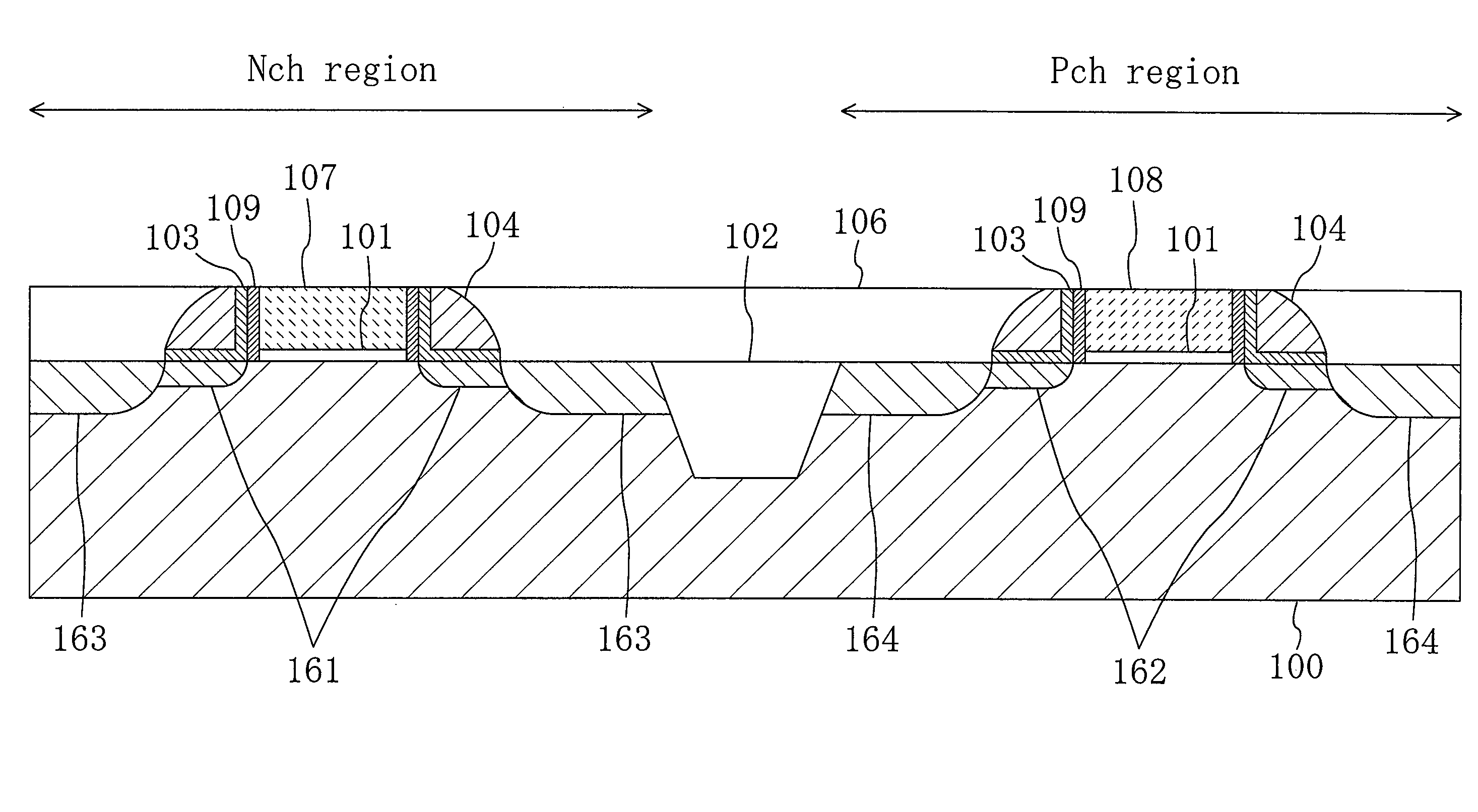
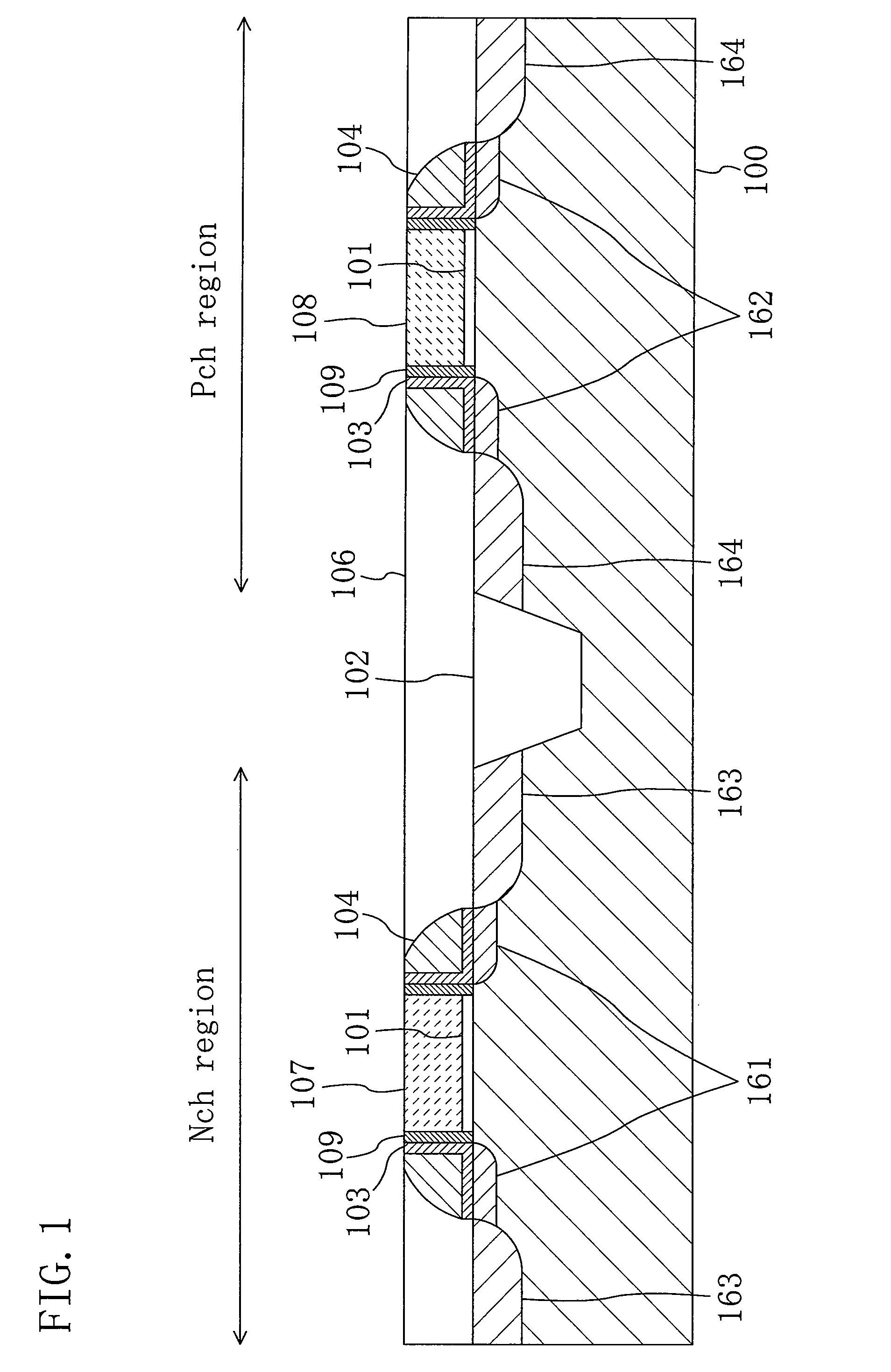
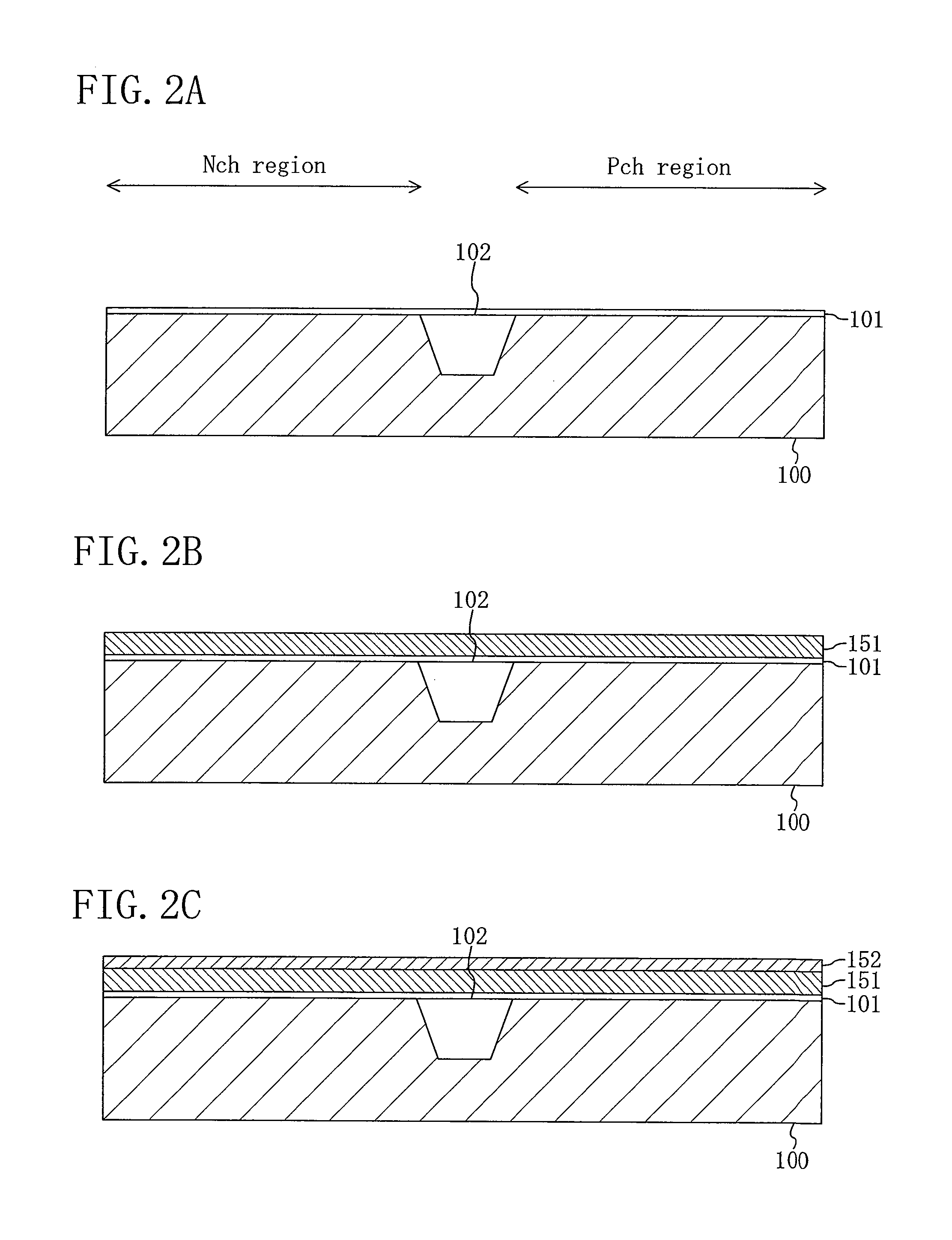
[0103]In Embodiment 1, the metal film 159 is deposited (FIG. 8A) at which time the insulating film 106 covering the source / drain regions 163 and 164 is not removed. However, in the present variation, before depositing the metal film 159, the insulating film 106 is removed to form silicided electrodes using the metal film 159, and at the same time, to silicide the surface portions of the source / drain regions 163 and 164. In forming the silicided electrodes, gate electrodes may be fully silicided to form FUSI electrodes as in the case of Embodiment 1. However, an effect similar to that of Embodiment 1 can be achieved by siliciding only surface portion or surface portions of one or both of the gate electrodes of the N-channel transistor and the P-channel transistor. In other words, it may not be required to fully silicide the gate electrodes to achieve the effect similar to that of Embodiment 1. This configuration can be achieved by adjusting, for exampl...

embodiment 2

Second Variation of Embodiment 2

[0131]In Embodiment 2, the metal film 159 is deposited (FIG. 11B) at which time the insulating film 106 covering the source / drain regions 163 and 164 is not removed. However, in the present variation, before depositing the metal film 159, the insulating film 106 is removed to form silicided electrodes using the metal film 159, and at the same time, to silicide the surface portions of the source / drain regions 163 and 164. In forming the silicided electrodes, gate electrodes may be fully silicided to form FUSI electrodes as in the case of Embodiment 2. However, an effect similar to that of Embodiment 2 can be achieved by siliciding only surface portion or surface portions of one or both of the gate electrodes of the N-channel transistor and the P-channel transistor. In other words, it may not be required to fully silicide the gate electrodes to achieve the effect similar to that of Embodiment 2. This configuration can be achieved by adjusting, for examp...

embodiment 3

Second Variation of Embodiment 3

[0156]In Embodiment 3, the metal film 159 is deposited (FIG. 14B) at which time the insulating film 106 covering the source / drain regions 163 and 164 is not removed. However, in the present variation, before depositing the metal film 159, the insulating film 106 is removed to form silicided electrodes using the metal film 159, and at the same time, to silicide the surface portions of the source / drain regions 163 and 164. In forming the silicided electrodes, gate electrodes may be fully silicided to form FUSI electrodes as in the case of Embodiment 3. However, an effect similar to that of Embodiment 3 can be achieved by siliciding only surface portion or surface portions of one or both of the gate electrodes of the N-channel transistor and the P-channel transistor. In other words, it may not be required to fully silicide the gate electrodes to achieve the effect similar to that of Embodiment 3. This configuration can be achieved by adjusting, for examp...


PUM


Abstract

A semiconductor device includes a gate electrode. The gate electrode includes a silicide layer obtained by siliciding porous silicon or organic silicon.

Description

CROSS-REFERENCE TO RELATED APPLICATION[0001]This is a continuation of PCT International Application PCT / JP2009 / 000231 filed on Jan. 22, 2009, which claims priority to Japanese Patent Application No. 2008-030982 filed on Feb. 12, 2008. The disclosures of these applications including the specifications, the drawings, and the claims are hereby incorporated by reference in its entirety.BACKGROUND[0002]The present disclosure relates to semiconductor devices such as Large Scale Integrated (LSI) Circuits and methods for fabricating the same.[0003]In recent years, as advanced semiconductor processes, attention has been drawn to processes for forming Fully Silicided (FUSI) electrode structures and metal gate electrode structures to improve the performance of transistors.[0004]A conventional method for forming a FUSI electrode structure will be described with reference to FIG. 18. FIG. 18 is a cross-sectional view of a transistor having a conventional, general FUSI electrode structure. First,...

Claims


Application Information

Patent Timeline
IPC IPC(8): H01L27/092H01L21/762H01L29/772
CPCH01L21/28097H01L21/823835H01L21/823842H01L29/4975H01L29/6656H01L29/6653H01L29/66545H01L29/66553H01L29/665
Inventor YOSHIDA, YOICHITSUZUMITANI, AKIHIKOKANEGAE, KENSHI
Owner PANASONIC CORP
Why Eureka
Try Eureka