Output buffer and source driver using the same

a source driver and output buffer technology, applied in the direction of differential amplifiers, amplifiers with semiconductor devices/discharge tubes, instruments, etc., can solve the problems of limited discharging ability, poor driving voltage provided to the pixel electrode, and restricted discharging current flowing through the conducted transistor mnb>6/b>, so as to increase the speed of switching, quick enhance the signal for driving, and save power consumption

Active Publication Date: 2010-04-01
HIMAX TECH LTD +1
View PDF8 Cites 6 Cited by
  • Summary
  • Abstract
  • Description
  • Claims
  • Application Information

AI Technical Summary

Benefits of technology

[0009]The present invention provides an output buffer that can quickly enhance the signal for driving by increasing the speeds of switching the output voltage to be

Problems solved by technology

The driving voltages provided to the pixel electrode are not as good as expected because of the panel loading effect and the process variation so that the source driver utilizes the output buffers to enhance the driving abilities of its driving channels.
However, the bias voltage Vb1 is a fixed voltage so that the dischargi

Method used


Image

  • Output buffer and source driver using the same
  • Output buffer and source driver using the same
  • Output buffer and source driver using the same

Examples


Embodiment Construction

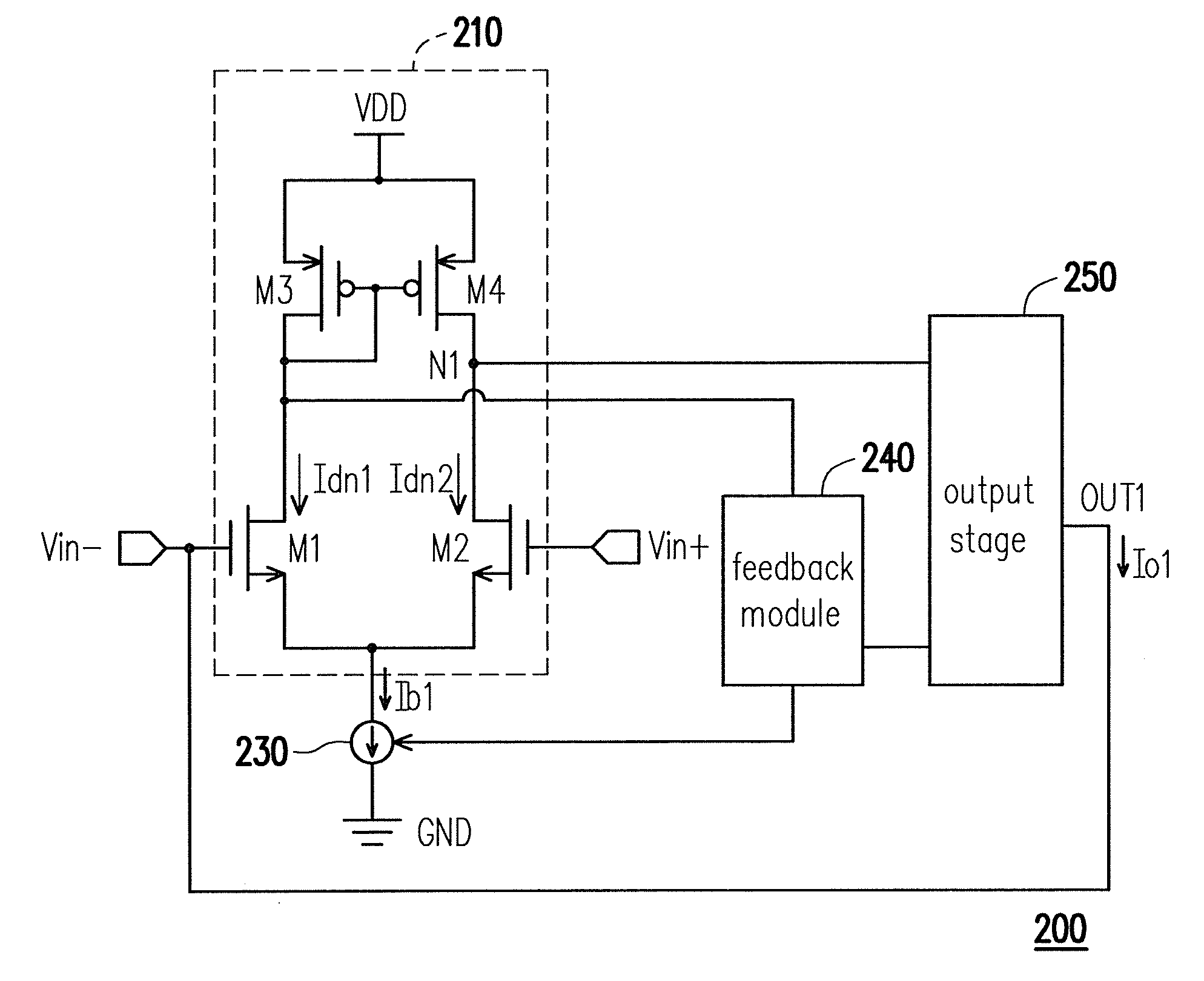
[0026]FIG. 2A is a diagram of an output buffer according to an embodiment of the invention. Referring to FIG. 2A, the output buffer 200 includes a differential input stage 210, a bias current source 230, a feedback module 240, and an output stage 250. The differential input stage 210 includes transistors M1 through M4, wherein in the embodiment, the transistors M1 and M2 are N-type transistors for composing N-type differential input pair, and the transistors M3 and M4 are P-type transistors. The differential input stage 210 has a first input terminal Vin− and a second input terminal Vin+ respectively receiving a first input signal and a second input signal, and has an output terminal N1. The bias current source 230 is coupled to the differential input stage 210 for providing a bias current Ib1 to the differential input stage 210 so that the differential input stage 210 can induce a first current Idn1 and a second current Idn2 based on the first input signal and the second input sign...


PUM


Abstract

An output buffer and a source driver for a display panel are provided. The output buffer includes a differential input stage, a bias current source, a feedback module, and an output stage. The differential input stage has a first input terminal and a second input terminal receiving a first input signal and a second input signal respectively, and a first output terminal. The bias module provides a bias current to the differential input stage. The output stage has a second output terminal coupled to the first input terminal for providing an output current to the second output terminal based on a signal of the first output terminal. The feedback module adjusts the bias current and the output current based on the first input signal and the second input signal. The output buffer has ability of switching the output voltage to be low level and high level in high-speed.

Description

BACKGROUND OF THE INVENTION[0001]1. Field of the Invention[0002]The present invention relates to an output buffer and a source driver using the same, and more particularly, to the output buffer enhancing the speeds of switching an output voltage of the output buffer to be low level and high level.[0003]2. Description of Related Art[0004]The source driver is an important component in the driving system of the display device, which is used for converting a digital video signal to a driving voltage and providing the driving voltage to a pixel electrode in association with a certain enabled scan line. The driving voltages provided to the pixel electrode are not as good as expected because of the panel loading effect and the process variation so that the source driver utilizes the output buffers to enhance the driving abilities of its driving channels.[0005]FIG. 1A is a circuit diagram of a conventional output buffer. Referring to FIG. 1, the output buffer 100a includes the transistors M...

Claims


Application Information

Patent Timeline
IPC IPC(8): G09G5/00
CPCG09G3/3614G09G2310/0291G09G3/3688
Inventor TSAI, CHIEN-HUNGWANG, JIA-HUILEE, CHING-CHUNG
Owner HIMAX TECH LTD
Why Eureka
Try Eureka