Semiconductor device and method of manufacturing the same

a semiconductor and capacitor technology, applied in the direction of semiconductor devices, semiconductor/solid-state device details, capacitors, etc., can solve the problems of difficult to provide a stable capacitance value, inappropriate structure or process of mim capacitors, etc., and achieve the effect of stable capacitance valu

Inactive Publication Date: 2010-04-08
RENESAS ELECTRONICS CORP
View PDF5 Cites 10 Cited by
  • Summary
  • Abstract
  • Description
  • Claims
  • Application Information

AI Technical Summary

Benefits of technology

[0014]According to the above-mentioned structure, the electrodes of the MIM capacitor is formed by the first high aspect via and the second high aspect via. Therefore, it is possible to prevent misalignment when the interconnects are formed on the vias. In this way, it is possible to maintain a constant distance between the electrodes and make the capacitance value of the MIM capacitor equal to the design value. As a result, it is possible to provide a stable capacitance value. In addition, it is possible to prevent a time dependent dielectric breakdown (TDDB) lifetime from being reduced.
[0016]According to the present invention, it is possible to provide a semiconductor device including a MIM capacitor with a stable capacitance value.

Problems solved by technology

In the multi-layer interconnect structure, achieving the appropriate structure or process for the MIM capacitor is an important technical issue.
As a result, the capacitance value of the MIM capacitor 12 is different from the design value and it is difficult to provide a stable capacitance value.

Method used


Image

  • Semiconductor device and method of manufacturing the same
  • Semiconductor device and method of manufacturing the same
  • Semiconductor device and method of manufacturing the same

Examples


Embodiment Construction

[0029]The invention will be now described herein with reference to illustrative embodiments. Those skilled in the art will recognize that many alternative embodiments can be accomplished using the teachings of the present invention and that the invention is not limited to the embodiments illustrated for explanatory purposes.

[0030]Hereinafter, exemplary embodiments of the invention will be described with reference to the accompanying drawings. In the drawings, the same components are denoted by the same reference numerals and description thereof will not be repeated.

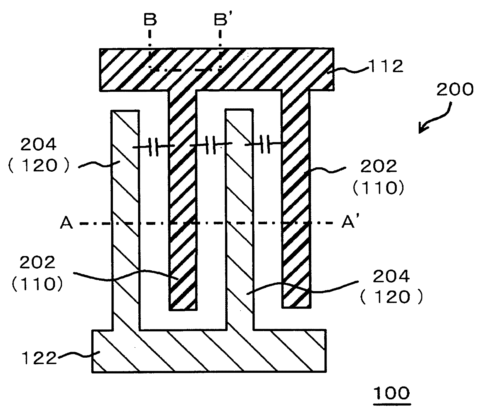
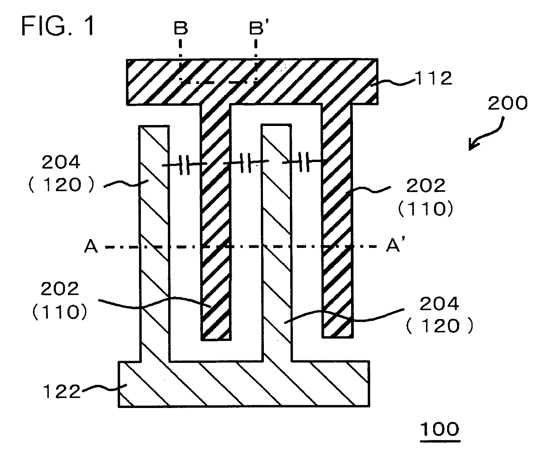
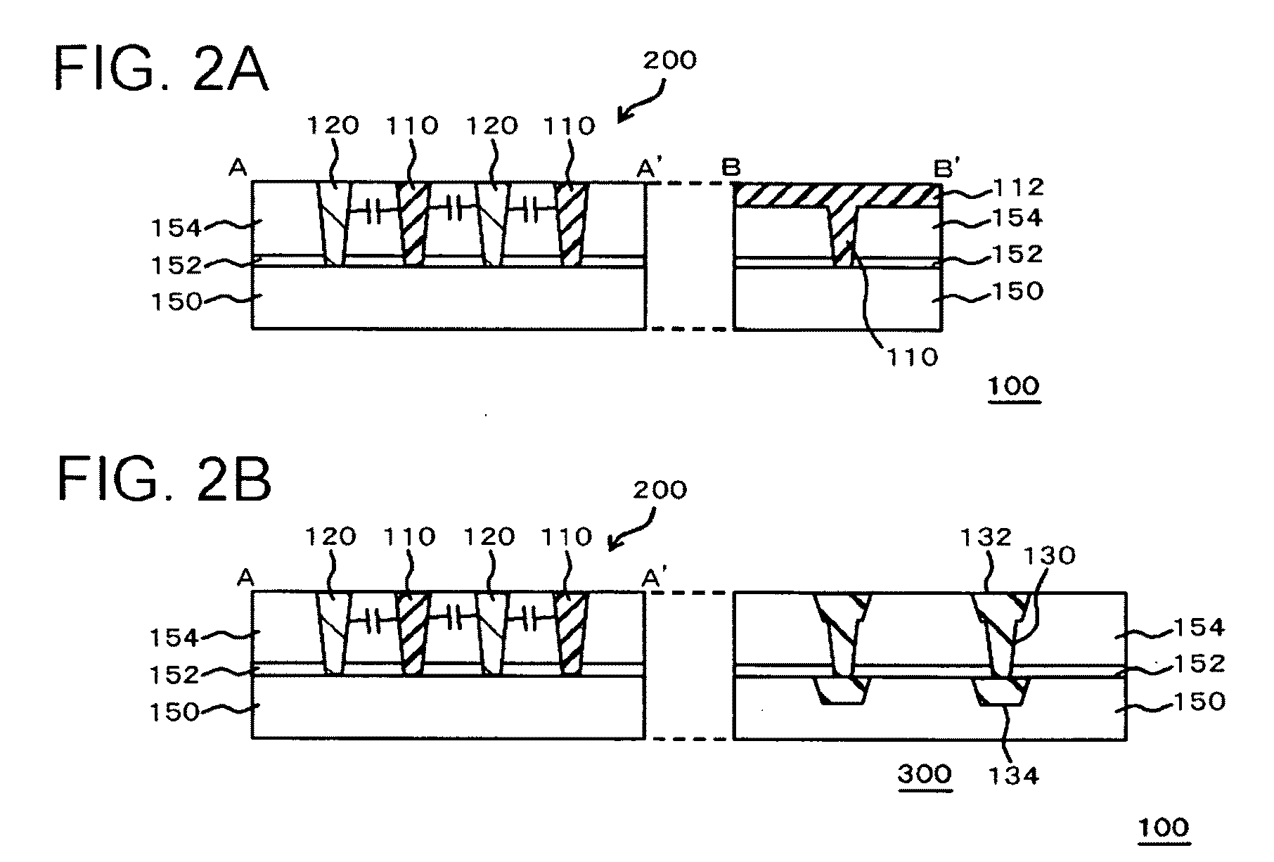
[0031]FIG. 1 is a plan view illustrating the structure of a semiconductor device according to an embodiment of the invention. FIGS. 2A and 2B are cross-sectional views illustrating the semiconductor device according to this embodiment. FIG. 2A is a cross-sectional view taken along the lines A-A′ and B-B′ of FIG. 1. FIG. 2B shows a cross section taken along the line A-A′ of FIG. 1 and another region 300 of a semiconductor ...


PUM


Abstract

A semiconductor device includes a MIM capacitor that includes an insulating film and a first electrode and a second electrode which are formed in the same layer in the insulating film and are facing to each other with the insulating film interposed therebetween. The first electrode and the second electrode respectively include a first high aspect via and a second high aspect via which extend as long as a length, in a stacked direction of the substrate, of a via and an interconnect provided on the via so as to be connected to the via formed in another region. A first potential and a second potential are respectively supplied to the first electrode and the second electrode.

Description

[0001]This application is based on Japanese patent application No. 2008-309088, the content of which is incorporated hereinto by reference.BACKGROUND[0002]1. Technical Field[0003]The present invention relates to a semiconductor device and a method of manufacturing the same, and more particularly, to a semiconductor device including a MIM capacitor and a method of manufacturing the same.[0004]2. Related Art[0005]In recent years, metal-insulator-metal (MIM) capacitors having a parasitic resistance and a parasitic capacitance significantly less than those of conventional MOS capacitors have been used as capacitor elements. In addition, a structure in which the MIM capacitor is incorporated into a logic device to form one chip has been developed. In order to achieve the structure, it is necessary to integrate the structures and the manufacturing processes of the two devices. In the logic device, a multi-layer interconnect structure has been generally used. In the multi-layer interconnec...

Claims


Application Information

Patent Timeline
Patent Type & Authority Applications(United States)
IPC IPC(8): H01L29/92H01L21/02
CPCH01L21/76804H01L21/76816H01L23/5223H01L28/90H01L2924/0002H01L2924/00
Inventor MATSUI, KOUJIROU
Owner RENESAS ELECTRONICS CORP
Why Eureka
Try Eureka