Check patentability & draft patents in minutes with Patsnap Eureka AI!

Buffer of semiconductor memory apparatus

a memory apparatus and buffer technology, applied in the direction of logic circuits, pulse techniques, and increasing modifications, etc., can solve the problems of reducing the operational reliability of the semiconductor memory apparatus, affecting the reliability of the buffer, and generating a small amount of curren

Inactive Publication Date: 2010-04-15
SK HYNIX INC
View PDF9 Cites 3 Cited by
  • Summary
  • Abstract
  • Description
  • Claims
  • Application Information

AI Technical Summary

Benefits of technology

[0013]In one embodiment, a buffer of a semiconductor memory apparatus includes a buffering section configured to generate an output signal by buffering an input signal; and a mismatch compensation section configured to generate a control voltage in correspondence with sizes of a second transistor of the same type as a first transistor constituting the buffering section, wherein the buffering section controls a transition time of the output signal in response to a level of the control voltage.
[0014]In another embodiment, a buffer of a semiconductor memory apparatus includes a buffering section configured to generate an output signal

Problems solved by technology

However, the buffer having this structure is vulnerable to process variation.
In general, as the size of the transistor that is turned on increases, the transistor outputs a large amount of current and as the size of the transistor decreases, the transistor outputs a small amount of current, such that the above-mentioned problem occurs.
When the transition time of the output signal ‘outb’ is shortened or lengthened, an internal circuit that receives the output signal ‘outb’ may not perform a normal operation, such that operational reliability of the semiconductor memory apparatus decreases.
As described above, only the process variation is regarded as a problem in operation of the buffer, but in the case of the buffer, a threshold voltage of the transistor varies by variation of a temperature and a voltage, such that an amount of current that is outputted from the transistor varies.

Method used


Image

  • Buffer of semiconductor memory apparatus
  • Buffer of semiconductor memory apparatus
  • Buffer of semiconductor memory apparatus

Examples


Embodiment Construction

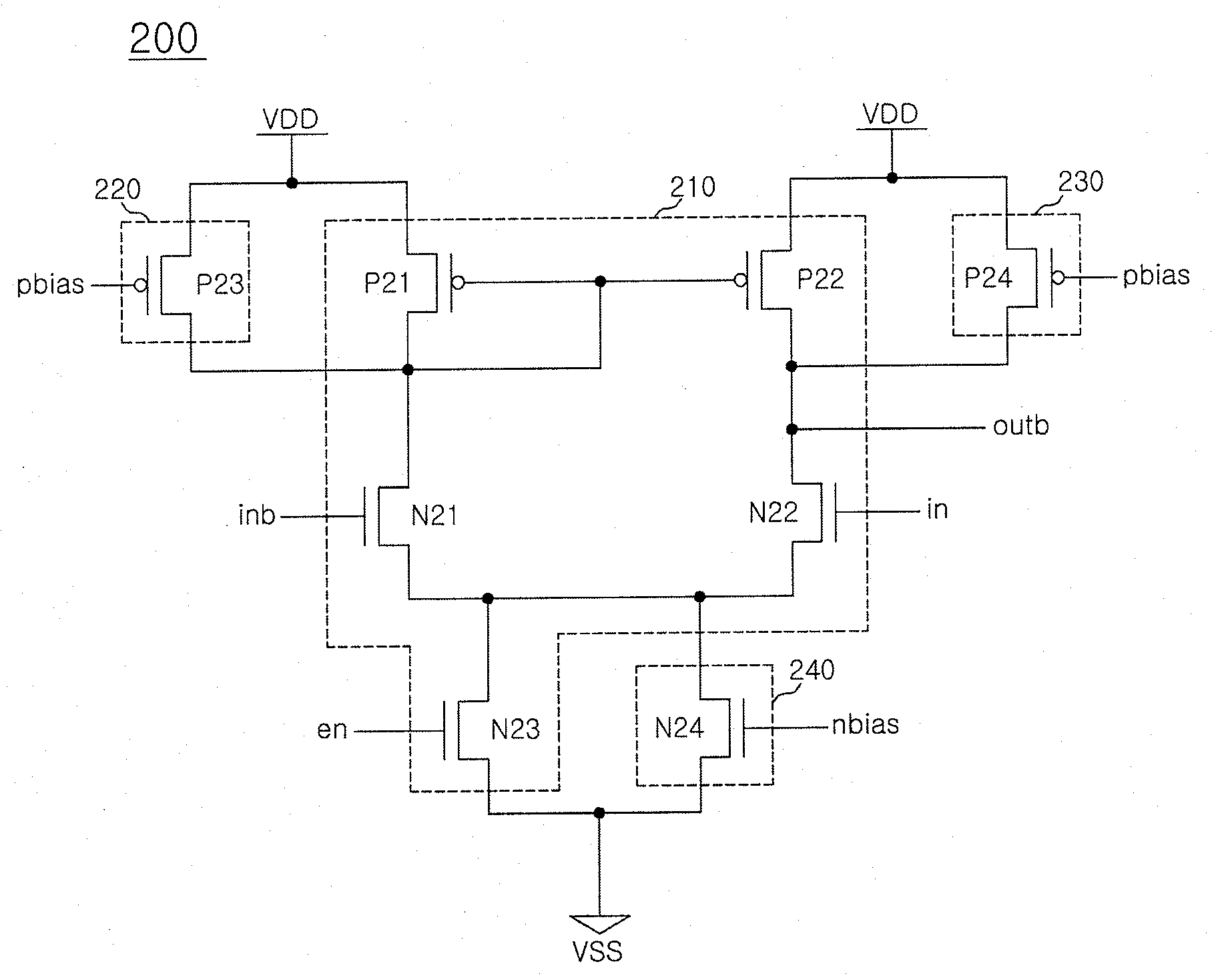
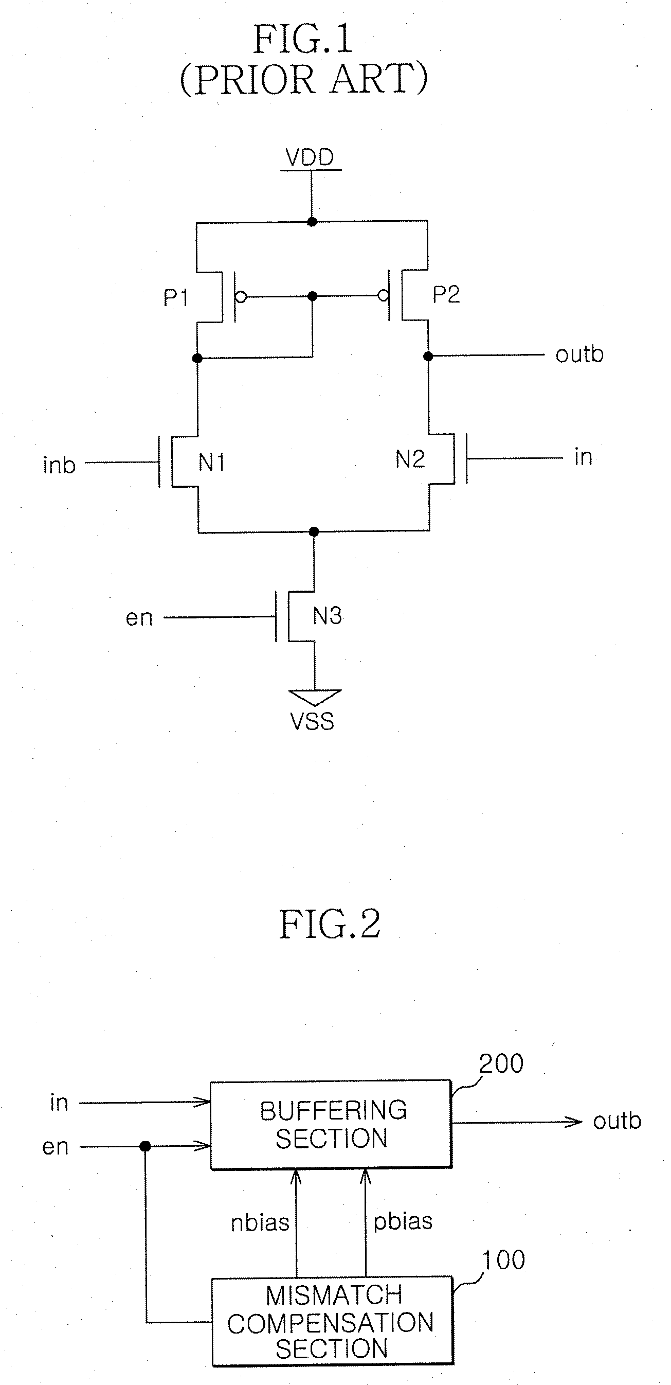
[0021]A buffer of a semiconductor memory apparatus according to one embodiment can be configured to include a mismatch compensation section 100 and a buffering section 200 as shown in FIG. 2.

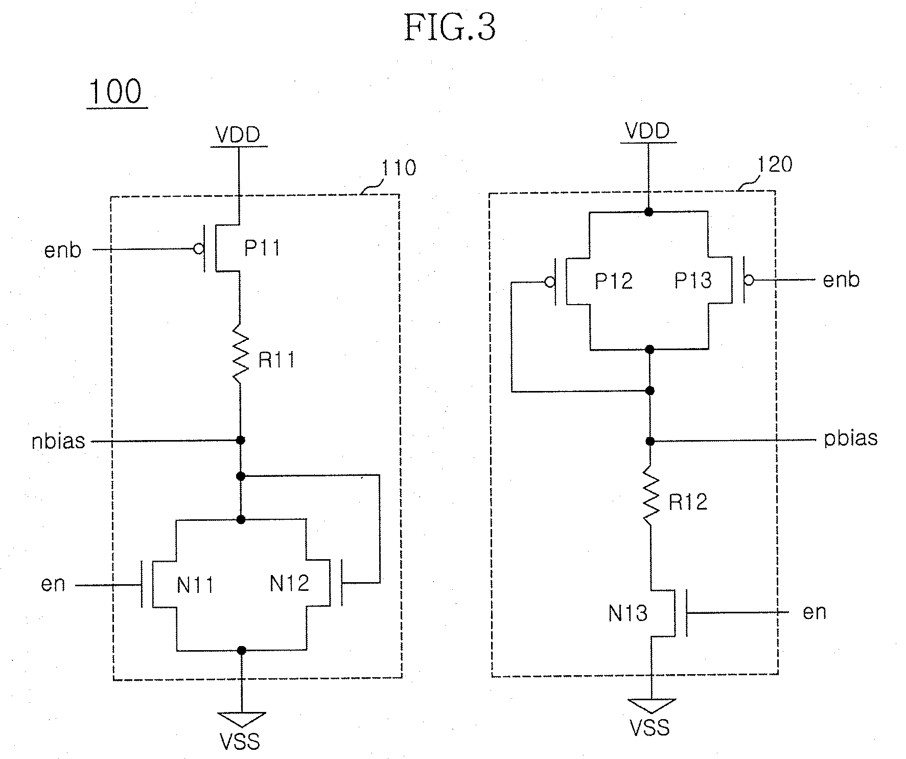
[0022]The exemplary mismatch compensation section 100 is configured to generate a control voltage in correspondence with a size of a transistor. At this time, the mismatch compensation section 100 can generate a first control voltage ‘nbias’ in correspondence with a size of an NMOS-type transistor. Further, the mismatch compensation section 100 can generate a second control voltage ‘pbias’ in correspondence with a size of a PMOS-type transistor. For example, the mismatch compensation section 100 can decrease a level of the first control voltage ‘nbias’ as the size of the NMOS-type transistor constituting the buffering section 200 increases and increase a level of the second control voltage ‘pbias’ as the size of the PMOS-type transistor constituting the buffering section 200 increases. In genera...


PUM


Abstract

A buffer of a semiconductor memory apparatus includes a buffering section configured to generate an output signal by buffering an input signal. A mismatch compensation section generates a control voltage in correspondence with sizes of a second transistor of the same type as a first transistor constituting the buffering section, wherein the buffering section controls a transition time of the output signal in response to a level of the control voltage.

Description

CROSS-REFERENCES TO RELATED PATENT APPLICATION[0001]The present application claims priority under 35 U.S.C 119(a) to Korean Application No. 10-2008-0100645, filed on Oct. 14, 2008, in the Korean Intellectual Property Office, which is incorporated herein by reference in its entirety as set forth in full.BACKGROUND[0002]1. Technical Field[0003]The embodiment described herein relates to a semiconductor memory apparatus and, more particularly, to a buffer of the semiconductor memory apparatus.[0004]2. Related Art[0005]A general buffer includes first to fifth transistors P1, P2, and N1 to N3 as shown in FIG. 1. The first transistor P1 is applied with an external voltage VDD at a source thereof. A gate of the second transistor P2 is connected to a gate of the first transistor P1 and is applied with the external voltage VDD at a source thereof. The third transistor N1 receives an inverted input signal ‘inb’ at a gate thereof and a drain of the third transistor N1 is connected to the gate a...

Claims


Application Information

Patent Timeline
IPC IPC(8): H03K19/094H03K19/0175
CPCH03K19/018528G11C5/14G11C7/10
Inventor BYEON, SANG JIN
Owner SK HYNIX INC
Features
  • R&D
  • Intellectual Property
  • Life Sciences
  • Materials
  • Tech Scout
  • Unparalleled Data Quality
  • Higher Quality Content
  • 60% Fewer Hallucinations
Learn More