LED pixel driving circuit

Inactive Publication Date: 2010-04-15
INNOLUX CORP
5 Cites 3 Cited by

AI-Extracted Technical Summary

Problems solved by technology

The 2T1C structure is simple, but it may cause the non-uniformity of brightness over the panel.
Therefore, different power supply voltages Vdd would cause the emit...

Benefits of technology

[0007]With embodiments described in the specification, the present invention, in one aspect, provides a pixel driving circuit for OLED, wherein the storage capacitor is connected to a power supply via a switching circuit, and the storage capacitor is connected to a reference voltage source via another ...

Abstract

An OLED pixel driving circuit includes a storage capacitor, a first switching circuit, and a driving element. The storage capacitor has a first node and a second node, where the second node receives Data voltage in a first period, and the first node receives reference voltage in a second period within the first period. The first switching circuit isolates the first node from a fixed voltage source in the first period, and connects the first node to the fixed voltage source to provide a fixed voltage to the first node after the end of the first period. The driving element outputs a driving current independently of the fixed voltage.

Application Domain

Cathode-ray tube indicatorsInput/output processes for data processing

Technology Topic

Driven elementVoltage reference +7

Image

  • LED pixel driving circuit
  • LED pixel driving circuit
  • LED pixel driving circuit

Examples

  • Experimental program(1)

Example

[0016]Reference will now be made in detail to the preferred embodiments of the present invention, examples of which are illustrated in the accompanying drawings. While the invention will be described in conjunction with the preferred embodiments, it will be understood that they are not intended to limit the invention to these embodiments, particularly those sizes, scales, and relative positions shown in the drawings.
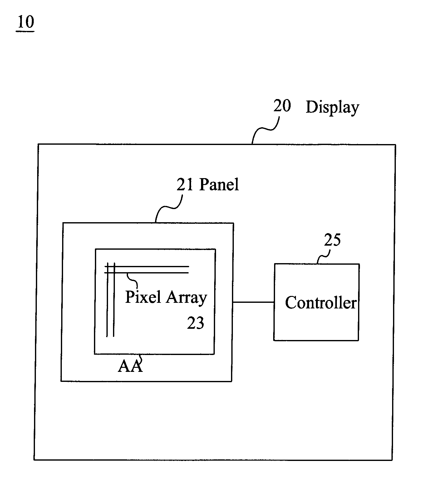
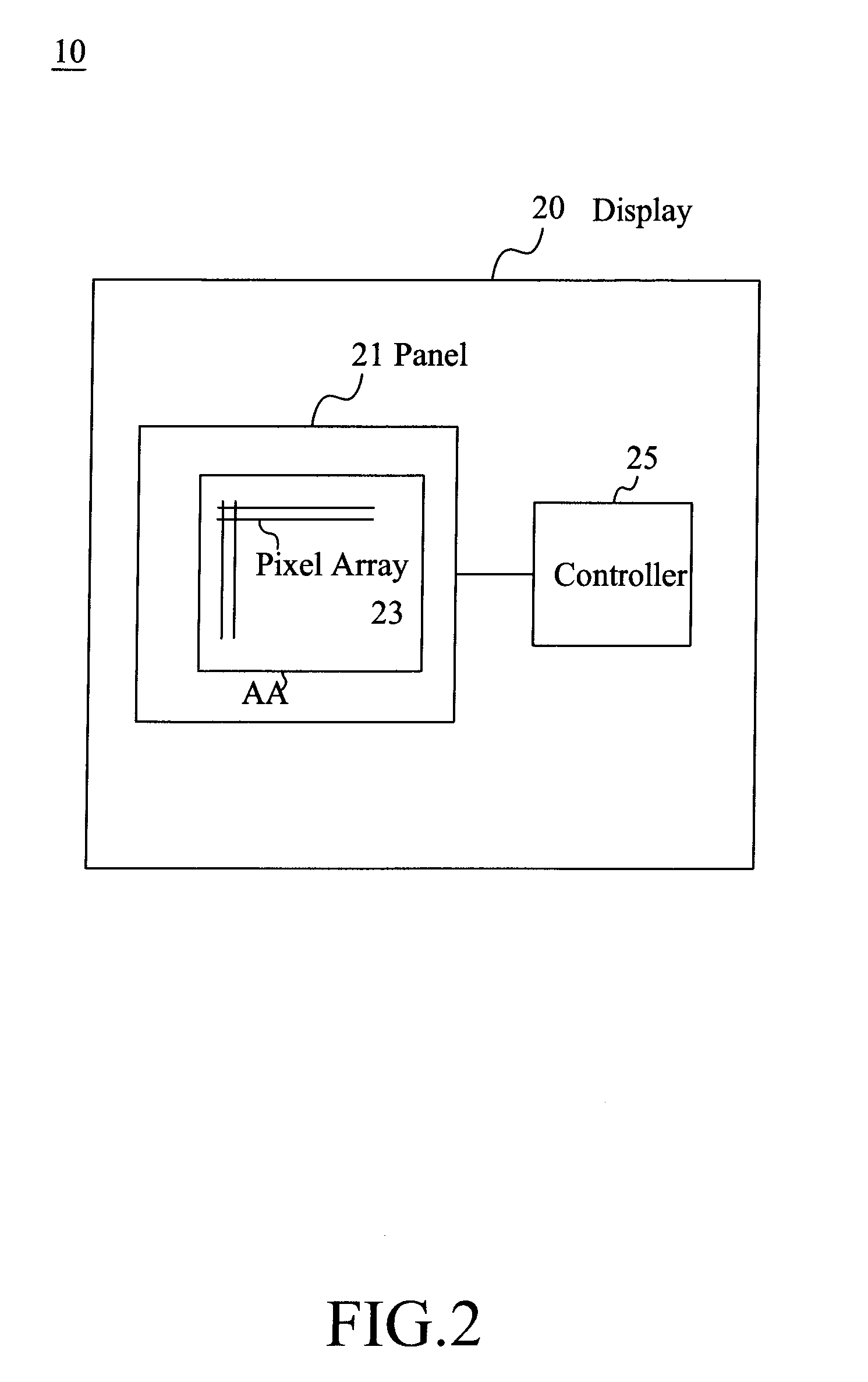
[0017]FIG. 2 is a block diagram of an electronic device 10 according to an embodiment of the present invention. In this embodiment, the electronic device 10 could be a TV, a mobile phone, a digital camera, a personal digital assistant (PDA), a notebook computer, a desktop computer, a television, a global positioning system (GPS), a car media player, an avionics display, a digital photo frame, a portable video player, etc. In this embodiment, the electronic device 10 includes an AMOLED display 20 and a controller 25. The AMOLED display 20 has a panel 21, and the panel 21 has an Active Area (AA) 22. A pixel array 23 in Active Area 22 has a plurality of data lines and scan lines. The controller 25 controls the operation of pixel driving circuits of the pixel array 23 to present images on the display 20.
[0018]As shown in FIG. 3a, the pixel driving circuit 300a includes a storage capacitor Cst, a first switching circuit 310, a second switching circuit 320, a third switching circuit 330, and a driving element 305. The first switching circuit 310 is disposed between the first node A of the capacitor Cst and a fixed voltage source Vdd of the panel 21. Note that the fixed voltage source Vdd can output a voltage around 5V, for example. However, the actual voltage received by a pixel from the fixed voltage source Vdd would depend on the pixel position and thus is difficult to ascertain. The second switching circuit 320 is disposed between the second node B of the capacitor Cst and a data line Data of the panel 21. The third switching circuit 330 is disposed between the first node A of the capacitor Cst and a reference voltage source Vref of the panel 21. The driving element 305 could be a PMOS transistor, disposed between the fixed voltage source Vdd and the emitting device EL. As shown, the has a source connected to the fixed voltage source Vdd, a gate coupled to the second node B, and a drain connected to the emitting device EL.
[0019]Also as shown in FIG. 3a, the storage capacitor Cst, the first switching circuit 310, the second switching circuit 320, and the driving element 305 are all disposed within Active Area (AA) of the panel 21. The third switching circuit 330 is disposed outside Active Area (AA), but in the peripheral area of the panel 21. Note that one switching circuit 330 can support a number of pixels.
[0020]In an embodiment, the fixed voltage source Vdd is independent of the reference voltage source Vref on the panel 21. That is, there is no direct electrical connection between the fixed voltage source Vdd and the reference voltage source Vref. For example, the flexible PCB (not shown) for the pixel driving circuit 300a has different contact pins for the fixed voltage source Vdd and the reference voltage source Vref.
[0021]Operations of the pixel driving circuit 300a will be described in the following. In the first period P1, when the first switching signal CS1 goes from short level to open level, the first switching 310 is turned open to isolate the first node A of the capacitor Cst from the fixed voltage source Vdd of the panel 21. Then when the second switching signal CS2 goes from open level to short level, the second switching 320 is turned short to connect the second node B of the capacitor Cst to the data line Data of the panel 21.
[0022]The second period P2 starts after the beginning of the first period P1. Then in the second period P2, when the third switching signal CS3 goes from open level to short level, the third switching 330 is turned short to connect the first node A of the capacitor Cst to the reference voltage source Vref of the panel 21, and the first node A receives the reference voltage from the reference voltage source Vref. In this embodiment, the second period P2 starts at least 50 ns later after the beginning of the first period P1, and the second period P2 lasts at least 0.5 μs. Then in response to a timing signal (not shown), the data line Data writes the data voltage Vdata to the second node B, so the stored voltage across the storage capacitor Cst is (Vdata−Vref).
[0023]When the second period P2 comes to the end and the third switching signal CS3 goes from short level to open level, the third switching circuit 330 is turned open. Next, the first period P1 comes to the end, and when the first switching signal CS1 goes from open level to short level and the second switching signal CS2 goes from short level to open level, the second switching circuit 320 is turned open but the first switching circuit 310 is turned short. Thus the first node A is connected to the fixed voltage source Vdd, and the voltage at the first node A become Vdd. To maintain the stored voltage across the storage capacitor Cst, the voltage at the second node B becomes (Vdd+Vdata−Vref). In this embodiment, the first period P1 ends at least 50 ns later after the end of the second period P2.
[0024]The gate of PMOS transistor 305 is coupled to the second node B, so the gate voltage is equal to (Vdd+Vdata−Vref). The source of PMOS transistor 305 is coupled to the fixed voltage source Vdd to have the source voltage equal to Vdd, so the gate-source voltage Vgs of PMOS transistor 305 is equal to (Vdata−Vref), which is independent of the fixed voltage Vdd. Accordingly, the current outputted from the drain of PMOS transistor 305 would not be affected by the voltage drop of the fixed voltage Vdd. As a result, the brightness uniformity is improved.
[0025]Compared with the pixel driving circuit 300a, the pixel driving circuit 300b shown in FIG. 3b has a storage capacitor Cst, a first switching circuit 310, a second switching circuit 320, a third switching circuit 330, and a driving element 305 all disposed in Active Area (AA) of the panel 21. Except that, the pixel driving circuit 300a and the pixel driving circuit 300b have similar structure and operations. Therefore the details of the pixel driving circuit 300b are omitted herein.
[0026]FIG. 3c and FIG. 3d show other embodiments. Compared with the embodiments shown in FIG. 3a and FIG. 3b, the switching circuit 330c in FIG. 3c further includes a fourth switching circuit 340 disposed between the driving element 305 and the emitting device EL. In response to a fourth switching signal CS4, the fourth switching circuit 340 is turned open or short. In this embodiment, the fourth switching signal CS4 and the aforementioned first switching signal CS1 are the same one. When the first switching circuit 310 is turned short, the fourth switching circuit 340 is turned short too; when the first switching circuit 310 is turned open, the fourth switching circuit 340 is turned open too. In addition, the first switching circuit 310 and the third switching circuit 330 are both disposed outside Active Area (AA).
[0027]Compared with the embodiments shown in FIG. 3a and FIG. 3b, the switching circuit 330d in FIG. 3d further includes a fifth switching circuit 350 disposed between the driving element 305 and the fixed voltage source Vdd. In response to a fifth switching signal CS5, the fifth switching circuit 350 is turned open or short. In this embodiment, the fifth switching signal CS5 and the aforementioned first switching signal CS1 are the same one. When the first switching circuit 310 is turned short, the fifth switching circuit 350 is turned short too; when the first switching circuit 310 is turned open, the fifth switching circuit 350 is turned open too. In addition, as shown in FIG. 3d, the first switching circuit 310 and the third switching circuit 330 are both disposed outside Active Area (AA).
[0028]As for the pixel driving circuit 300e in FIG. 3e, the first switching circuit 310 includes a PMOS transistor; the second switching circuit 320 includes a NMOS transistor; the third switching circuit 330 includes a NMOS transistor; and the driving element 305 includes a PMOS transistor. However, those skilled in the art should understand that the present invention is not limited to these embodiments.
[0029]As shown in FIG. 3e, PMOS transistor 310 is disposed between the first node A of the capacitor Cst and the fixed voltage source Vdd of the panel 21. The source of PMOS transistor 310 is connected to the fixed voltage source Vdd, the gate is coupled to the first scan line Scan 1, and the drain is coupled to the first node A.
[0030]NMOS transistor 320 is disposed between the second node B of the capacitor Cst and the data line Data of the panel 21. The drain of NMOS transistor 320 is connected to the data line Data, the gate is coupled to the first scan line Scan 1, and the source is coupled to the second node B.
[0031]NMOS transistor 330 is disposed between the first node A of the capacitor Cst and the reference voltage source Vref of the panel 21. The drain of NMOS transistor 330 is connected to the reference voltage source Vref, the gate is coupled to the second scan line Scan 2, and the source is coupled to the first node A.
[0032]In addition, in the embodiment of FIG. 3e, PMOS transistor 310, NMOS transistor 320, and PMOS transistor 305 are disposed in Active Area (AA) of the panel 21. But NMOS transistor 330 is disposed outside Active Area (AA). Instead, NMOS transistor 330 is disposed in the peripheral area of the panel 21. This type of arrangement is also referred to as “3T1C” structure. Note that one NMOS transistor 330 can support more than one pixel. Moreover, PMOS transistor 310, NMOS transistor 320, NMOS transistor 330, and PMOS transistor 305 could be implemented as thin film transistors (TFT).
[0033]In the embodiment of FIG. 3f, PMOS transistor 310, NMOS transistor 320, NMOS transistor 330 and PMOS transistor 305 are disposed in Active Area (AA) of the panel 21. This type of arrangement is also referred to as “4T1C” structure. Except that, the pixel driving circuit 300f and the pixel driving circuit 300e have similar structure and operations. Therefore the details of the pixel driving circuit 300f are omitted herein.
[0034]Operations of the pixel driving circuit 300e or the circuit 300f will be explained in greater detail as follows. At first, in the first period P1, the first scan line SCAN 1 is pulled high to output a first scan signal to gates of PMOS transistor 310 and of NMOS transistor 320, to make PMOS transistor 310 off but to make NMOS transistor 320 on.
[0035]After the beginning of the first period P1, the second scan line SCAN 2 in the second period P2 is pulled high to output a second scan signal to the gate of NMOS transistor 330, to make NMOS transistor 330 on, so the first node A receives the reference voltage from the reference voltage source Vref. Then in response to a timing signal (not shown), the data line Data writes the data voltage Vdata to the second node B, so the stored voltage across the storage capacitor Cst is (Vdata−Vref).
[0036]Next, the second scan line SCAN 2 is pulled low and the second period P2 comes to the end. After that, the first scan line SCAN 1 is also pulled low and the first period P1 comes to the end too. Meanwhile, NMOS transistor 320 is turned off and the PMOS transistor 310 is turned on, so that the first node A is connected to the fixed voltage source Vdd, and the voltage at the first node A becomes Vdd. But to maintain the stored voltage across the storage capacitor Cst, the voltage at the second node B becomes (Vdd+Vdata−Vref).
[0037]The gate of PMOS transistor 305 is coupled to the second node B, so the gate voltage is equal to (Vdd+Vdata−Vref). The source of PMOS transistor 305 is coupled to the fixed voltage source Vdd to have the source voltage equal to Vdd, so the gate-source voltage Vgs of PMOS transistor 305 is equal to (Vdata−Vref), which is independent of the fixed voltage Vdd. Accordingly, the current outputted from the drain of PMOS transistor 305 would not be affected by the voltage drop of the fixed voltage Vdd. As a result, the brightness uniformity could be improved.
[0038]While this invention has been described with reference to the illustrative embodiments, these descriptions should not be construed in a limiting sense. Various modifications of the illustrative embodiment, as well as other embodiments of the invention, will be apparent upon reference to these descriptions. It is therefore contemplated that the appended claims will cover any such modifications or embodiments as falling within the true scope of the invention and its legal equivalents.

PUM

no PUM

Description & Claims & Application Information

We can also present the details of the Description, Claims and Application information to help users get a comprehensive understanding of the technical details of the patent, such as background art, summary of invention, brief description of drawings, description of embodiments, and other original content. On the other hand, users can also determine the specific scope of protection of the technology through the list of claims; as well as understand the changes in the life cycle of the technology with the presentation of the patent timeline. Login to view more.

Similar technology patents

Method for manufacturing low-carbon and low-silicon steel

ActiveCN103627853Aeasy to implementReduce oxidation
Owner:SGIS SONGSHAN CO LTD

System and method for accurate measuring transmission effect of P2P stream media netwrok for video / audio programs

InactiveCN101094107ATo achieve a wide range of applicationseasy to implement
Owner:WANGSHITIANYUAN IT TECH

Classification and recommendation of technical efficacy words

  • easy to implement

Intelligent video monitoring method and system thereof

InactiveCN101635835AEasy to implementEasy system expansion
Owner:SHENZHEN XINYI TECH CO LTD

Voice call routing by dynamic personal profile

InactiveUS7653191B1less laboreasy to implement
Owner:MICROSOFT TECH LICENSING LLC
Why Eureka
Try Eureka