Release film for semiconductor resin molds

a technology of semiconductor resin and release film, which is applied in the direction of thin material processing, semiconductor devices, electrical devices, etc., can solve the problems of high amount of gas and low viscosity material formed from the molten mold resin under a high pressure, and insufficient releasability cannot be obtained, so as to prevent mold contamination, effectively suppress mold contamination, and low gas permeability

Inactive Publication Date: 2010-04-22
AGC INC
View PDF5 Cites 13 Cited by
  • Summary
  • Abstract
  • Description
  • Claims
  • Application Information

AI Technical Summary

Benefits of technology

[0028]According to the present invention, a release film can be provided which has extremely low gas permeability as compared with conventional ones and can substantially prevent mold contamination by a mold resin. Further, a gas permeability required for the release film to effectively suppress the mold contamination, is defined by a gas permeability rate corresponding more realistically to a low viscosity material from a resin as a mold contaminant. Further, according to the present invention, a release film having a higher releasability from a mold resin can be provided. Further, the release film of the present invention is excellent in mold obsequence property.
[0029]Therefore, by using the release film of the present invention in a molding step of the semiconductor resin, mold contamination is extremely low, and the number of times of mold cleaning can be reduced substantially, whereby it is possible to remarkably improve the production efficiency for molding a resin of a semiconductor element.

Problems solved by technology

On the other hand, along with a strong demand for improvement of productivity of a semiconductor package, there is a problem such that since the resin adheres to the mold, the contaminated mold needs to be often cleaned, or when a sealing resin having a low shrinkage corresponding to a large package is used, sufficient releasability cannot be obtained even if a releasing agent is added.
As a result, in the step of molding a resin for the semiconductor element, the amount of gas and low viscosity material formed from the molten mold resin under a high temperature environment increases, and the gas and low viscosity material permeating through the above release film for molds contact the mold having a high temperature, whereby the mold contamination becomes intense.
Further, covering the mold surface with the release film is carried out by sucking and supporting the film thereon under vacuum, but a volatile component such as an oligomer in the film transfers to the covered side of the mold, whereby the mold contamination may sometimes be caused.
Thus, even though the release film is used in such a manner, the side of the mold covered with the film, tends to be easily contaminated.
Further, once the contamination is caused, the molding step for the semiconductor is required to be stopped for cleaning, and such leads to a problem such that the production efficiency of the semiconductor decreases.
However, such a metal deposited layer is one to be used by direct physical contact to the mold surface, and a metal powder tends to be released from the film surface or a broken section of the film, whereby its use for a molding step of the semiconductor resin is limited.
Further, in Patent Documents 1 and 2, the gas permeability of the release film is defined by a permeation of carbon dioxide gas, but such is not valid as an index for evaluating the permeability of a low viscosity material, etc. from a resin, etc.
Further, the release film is now required to have higher releasability from the mold resin, but such was not considered for the above release film, and the releasability was insufficient.

Method used


Image

  • Release film for semiconductor resin molds
  • Release film for semiconductor resin molds
  • Release film for semiconductor resin molds

Examples


example 1

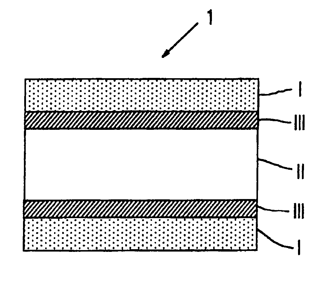
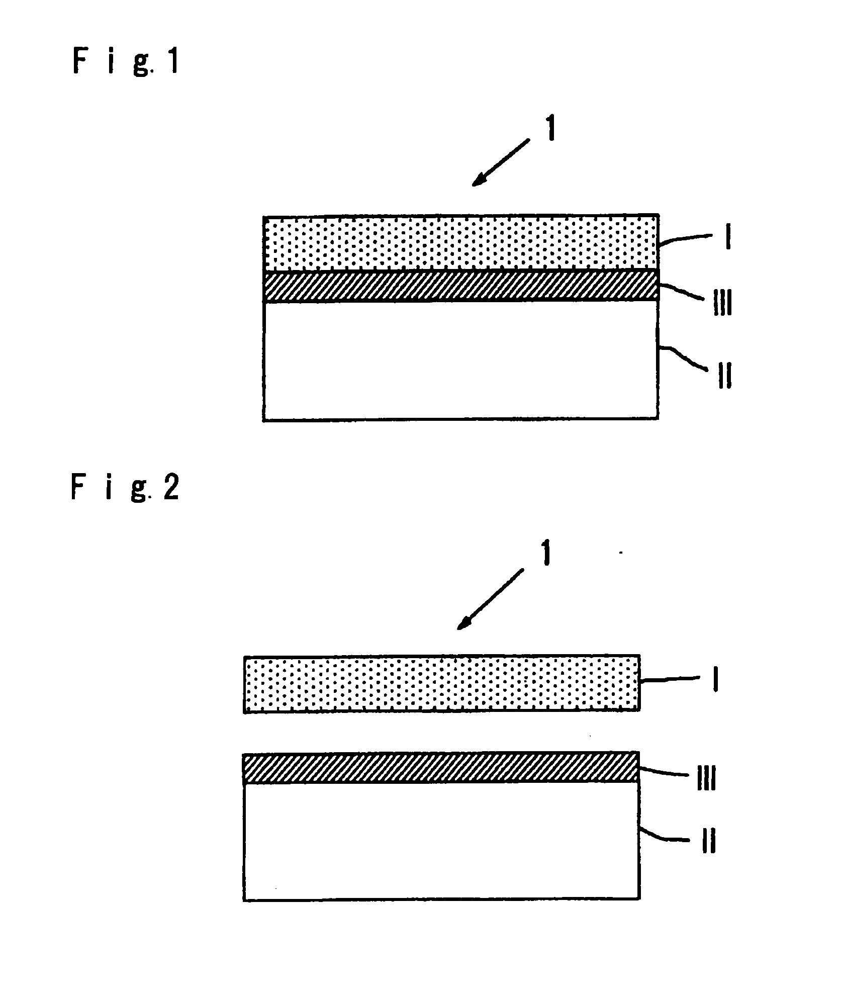
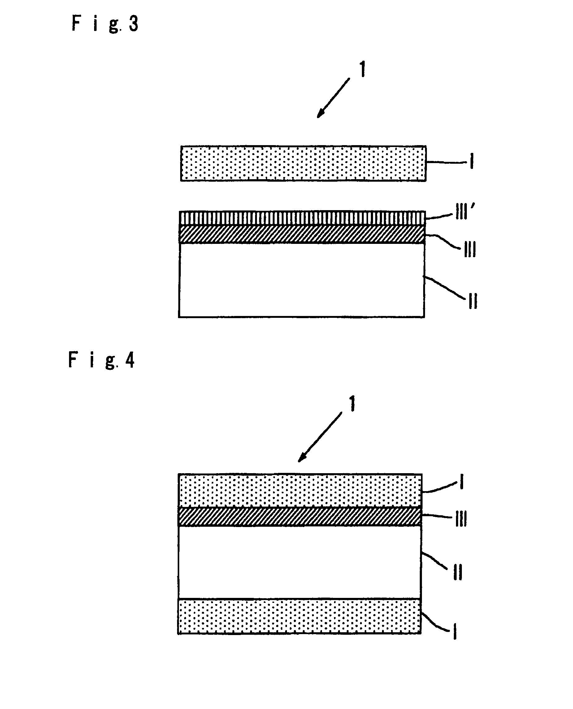
[0075](1) As the release layer (I), an ETFE film (manufactured by Asahi Glass Company, Limited, tradename: FLUON ETFE) having a thickness of 12 μm was used. One side (surface (surface to be bonded) facing a support layer) of the ETFE film was treated by corona discharge-treatment with a discharge amount of 40 W·min / m2 to improve the adhesion.

[0076]Further, a 12 μm polyethylene terephthalate film was used as the plastic support layer (II), and on one side of it, alumina was vapor-deposited as a metal oxide to form a gas restraint layer (III). Further, on it, a resin protection layer (III′) was coated to form a film (manufactured by Toppan Printing Co., Ltd., tradename, GX Film).

[0077](2) On the surface of the resin protection layer (III′) of the above film (GX Film), a polyester adhesive was applied to have a film thickness of 0.4 μm as dried, followed by drying, and as shown in FIG. 3, dry-laminating with a release layer (I) was carried out to obtain a release film (hereinafter refe...

example 2

[0084](1) A release film (hereinafter referred to as “release film 3”) was obtained in the same manner as in Example 1 except that a 12 μm ethylene / vinyl alcohol copolymer (manufactured by Kuraray Co., Ltd., tradename: EVAL EF-F) was used as the plastic support layer (II), and on its one side, aluminum was sputtered in a thickness of 10 nm to form a gas restraint layer (III), and no resin protection layer (III′) was formed.

[0085](2) With respect to the release film 3, the xylene gas permeability coefficient in an environment at 170° C. was calculated in the same manner as in Examples. Further, the peel strength was measured by a 180° C. peel test in the same manner as in Example 1.

[0086]The xylene gas permeability coefficient of the release film 3 was 1×10⁻¹⁶ (kmol·m / (s·m2·kPa)), the peel strength by a 180° peel test was 0 (N / m). The result is shown in Table 1.

[0087](3) Further, in the same manner as in Example 1, a mold shot was repeatedly carried out by using the release film 3, a...


PUM

PropertyMeasurementUnit
arithmetic surface roughnessaaaaaaaaaa
elongationaaaaaaaaaa
surface roughnessaaaaaaaaaa

Abstract

A process of sealing a semiconductor substrate by contacting the semiconductor substrate with a surface of a release layer (I) of a gas barrier release film that is in the form of a mold, which includes vacuum suction; injecting a sealing resin between the semiconductor substrate and the mold; and releasing said mold from said semiconductor substrate having said sealing resin present thereon, where the gas barrier release film has a release layer (I), which has excellent releasability; a plastic support layer (II) supporting the release layer; and a metal or a metal oxide gas restraint layer (III), present between the release layer and the support layer, where the gas barrier release film exhibits a xylene gas permeability of at most 5×10⁻¹⁵ (kmol m / (s·m2·kPa)) at 170° C., and a surface of said release layer (I) has an arithmetic surface roughness of from 0.15 to 3.5 μm, exhibiting a satin-finish.

Description

TECHNICAL FIELD[0001]The present invention relates to a release film for semiconductor resin molds, particularly a release film for semiconductor resin molds which can reduce mold contamination.BACKGROUND ART[0002]A semiconductor element (chip) is usually, for protection and blocking from an external environment (such as external air, contaminant, light, magnetism, high frequency wave or impulse), sealed with a resin (mold resin) and is mounted, on a substrate, in the form of a semiconductor package having the chip accommodated therein. Typically, the package is one formed by a transfer molding wherein a thermosetting resin (mold resin) such as an epoxy resin is melted by heating, and then, it is transferred in a mold where the semiconductor chip is set, followed by filling and curing. To the mold resin, a releasing agent is added in addition to a curing agent, a curing accelerator and a filler, to secure smooth releasability of the formed package from the mold.[0003]On the other ha...

Claims


Application Information

Patent Timeline
Patent Type & Authority Applications(United States)
IPC IPC(8): B29C45/14
CPCB29C33/68H01L21/566H01L2924/0002H01L2924/00Y10T428/3154Y10T428/31678Y10T428/31692H01L21/56
Inventor OKUYA, TAMAOARUGA, HIROSHIHIGUCHI, YOSHIAKI
Owner AGC INC
Why Eureka
Try Eureka