Release film for semiconductor resin molds

US20090053528A1Inactive Publication Date: 2009-02-26ASAHI GLASS CO LTD

Image

  • Release film for semiconductor resin molds
  • Release film for semiconductor resin molds
  • Release film for semiconductor resin molds

Examples


example 1

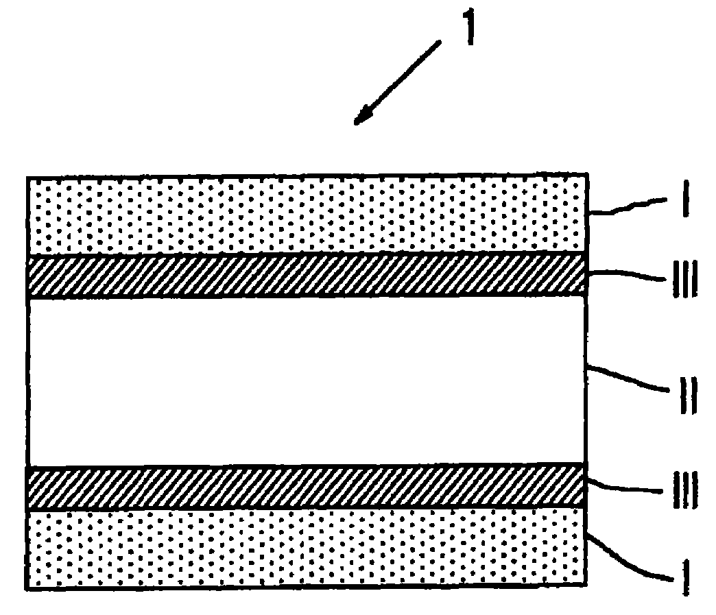
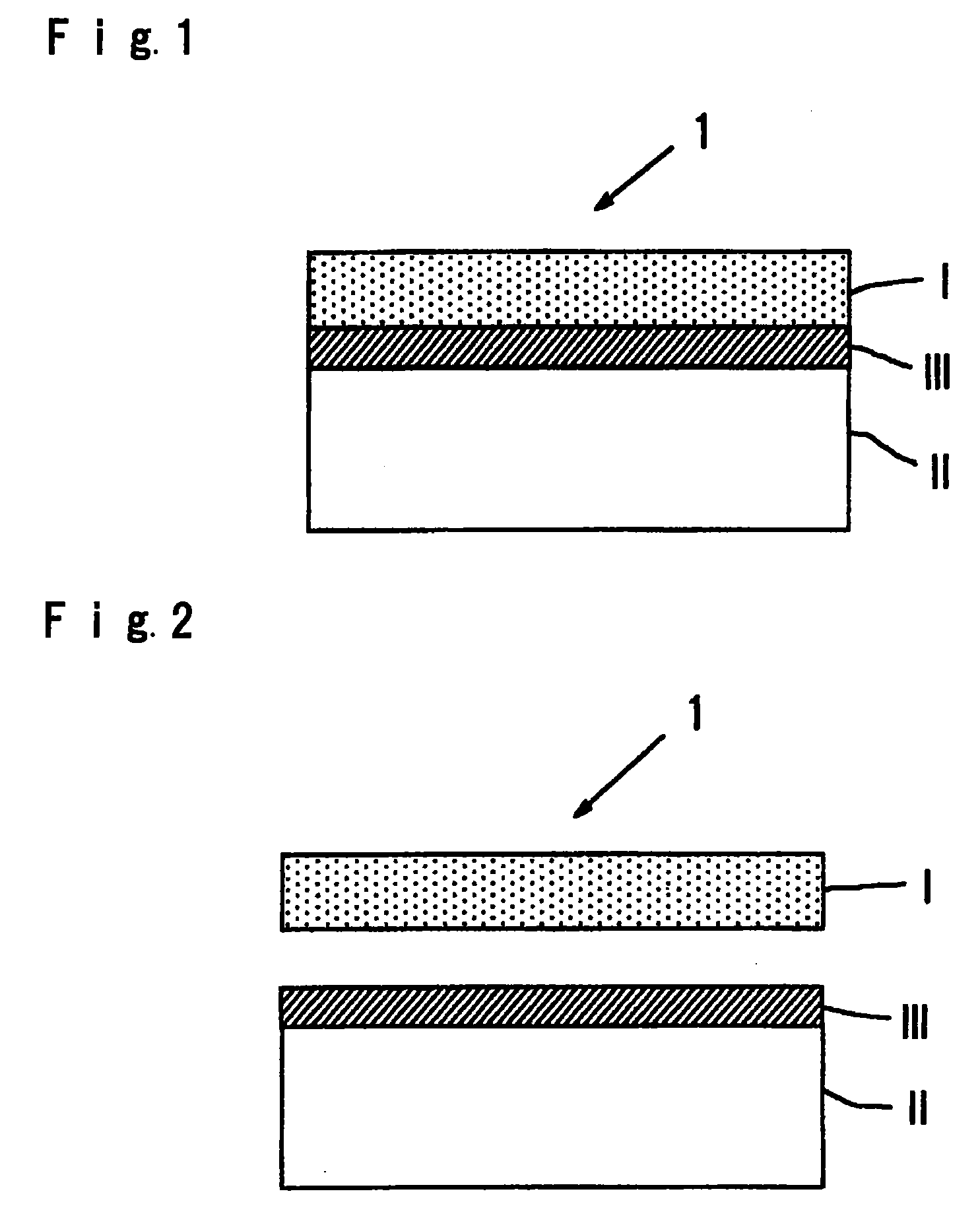
[0075](1) As the release layer (I), an ETFE film (manufactured by Asahi Glass Company, Limited, tradename: FLUON ETFE) having a thickness of 12 μm was used. One side (surface (surface to be bonded) facing a support layer) of the ETFE film was treated by corona discharge-treatment with a discharge amount of 40 W·min / m2 to improve the adhesion.

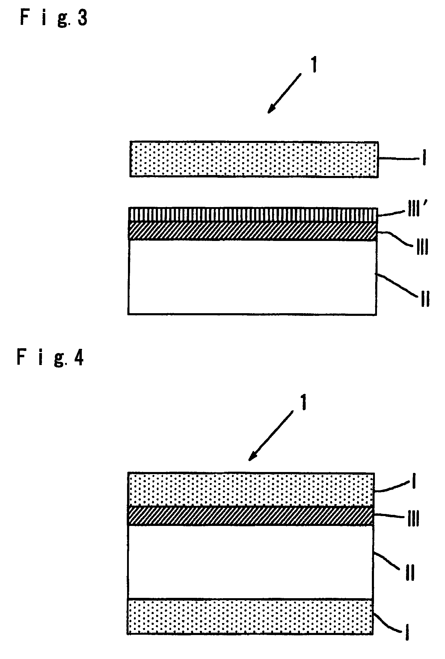
[0076]Further, a 12 μm polyethylene terephthalate film was used as the plastic support layer (II), and on one side of it, alumina was vapor-deposited as a metal oxide to form a gas restraint layer (III). Further, on it, a resin protection layer (III′) was coated to form a film (manufactured by Toppan Printing Co., Ltd., tradename, GX Film).

[0077](2) On the surface of the resin protection layer (III′) of the above film (GX Film), a polyester adhesive was applied to have a film thickness of 0.4 μm as dried, followed by drying, and as shown in FIG. 3, dry-laminating with a release layer (I) was carried out to obtain a release film (hereinafter refe...

example 2

[0084](1) A release film (hereinafter referred to as “release film 3”) was obtained in the same manner as in Example 1 except that a 12 μmethylene / vinyl alcohol copolymer (manufactured by Kuraray Co., Ltd., tradename: EVAL EF-F) was used as the plastic support layer (II), and on its one side, aluminum was sputtered in a thickness of 10 nm to form a gas restraint layer (III), and no resin protection layer (III′) was formed.

[0085](2) With respect to the release film 3, the xylene gas permeability coefficient in an environment at 170° C. was calculated in the same manner as in Examples. Further, the peel strength was measured by a 180° C. peel test in the same manner as in Example 1.

[0086]The xylene gas permeability coefficient of the release film 3 was 1×10⁻¹⁶ (kmol·m / (s·m2·kPa)), the peel strength by a 180° peel test was 0 (N / m). The result is shown in Table 1.

[0087](3) Further, in the same manner as in Example 1, a mold shot was repeatedly carried out by using the release film 3, an...


PUM

PropertyMeasurementUnit
Temperatureaaaaaaaaaa
Pressureaaaaaaaaaa
Pressureaaaaaaaaaa

Abstract

To provide a release film which has an extremely low gas permeability, an enormously small mold contamination by a mold resin and a high releasability.A gas barrier release film for semiconductor resin molds, comprising a release layer (I) having excellent releasability, a plastic support layer (II) supporting the release layer, and a gas restraint layer (III) made of a metal or a metal oxide, formed between the release layer and the support layer, and having a xylene gas permeability of at most 10−15 (kmol m / (s·m2·kPa)) at 170° C. The release layer (I) is preferably formed from a fluororesin such as an ethylene / tetrafluoroethylene copolymer, and a metal oxide layer is preferably a layer of an oxide such as an aluminum oxide, a silicon oxide or a magnesium oxide.

Description

TECHNICAL FIELD[0001]The present invention relates to a release film for semiconductor resin molds, particularly a release film for semiconductor resin molds which can reduce mold contamination.BACKGROUND ART[0002]A semiconductor element (chip) is usually, for protection and blocking from an external environment (such as external air, contaminant, light, magnetism, high frequency wave or impulse), sealed with a resin (mold resin) and is mounted, on a substrate, in the form of a semiconductor package having the chip accommodated therein. Typically, the package is one formed by a transfer molding wherein a thermosetting resin (mold resin) such as an epoxy resin is melted by heating, and then, it is transferred in a mold where the semiconductor chip is set, followed by filling and curing. To the mold resin, a releasing agent is added in addition to a curing agent, a curing accelerator and a filler, to secure smooth releasability of the formed package from the mold.[0003]On the other ha...

Claims


Application Information

Patent Timeline
26 Feb 2009
Publication
US20090053528A1
IPC
B32B15/04; B32B27/00
CPC
B29C33/68; H01L21/566; H01L2924/0002; H01L2924/00; Y10T428/3154; Y10T428/31678; Y10T428/31692; H01L21/56
Inventors
OKUYA, TAMAO; ARUGA, HIROSHI