Display device with chiplets and hybrid drive

Active Publication Date: 2010-05-20
GLOBAL OLED TECH
View PDF11 Cites 34 Cited by
  • Summary
  • Abstract
  • Description
  • Claims
  • Application Information

AI Technical Summary

Benefits of technology

[0012]The present invention has the advantage that, by providing a display device with chiplet drivers having row and column electrode connections for drivi

Problems solved by technology

However, a passive-matrix drive device is limited in the number of rows (or columns) that can be included in the device since the sequential nature of the row (or column) driving creates flicker.
If too many rows are included, the flicker can become perceptible.
Moreover, the currents necessary to drive an entire row (or column) in a display at a desired frame rate can be problematic and limits the physical size of a passive-matrix display.
Thin-film transistors (TFTs) made from amorphous or polycrystalline silicon are relatively large and have lower performance compared to conventional transistors made in crystalline silicon wafers.
Moreover, such thin-film devices typically exhibit local or large-area

Method used


Image

  • Display device with chiplets and hybrid drive
  • Display device with chiplets and hybrid drive
  • Display device with chiplets and hybrid drive

Examples


Embodiment Construction

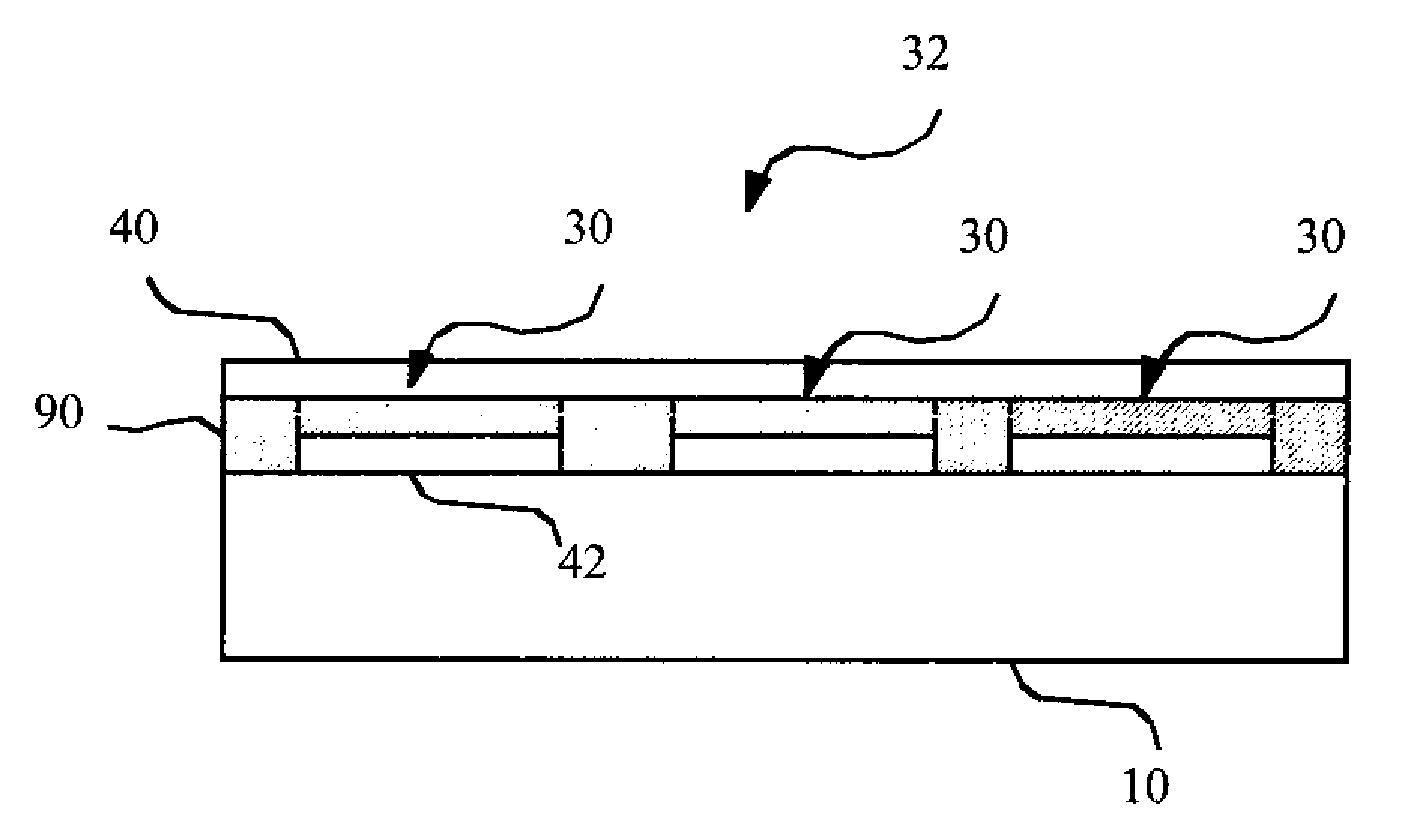
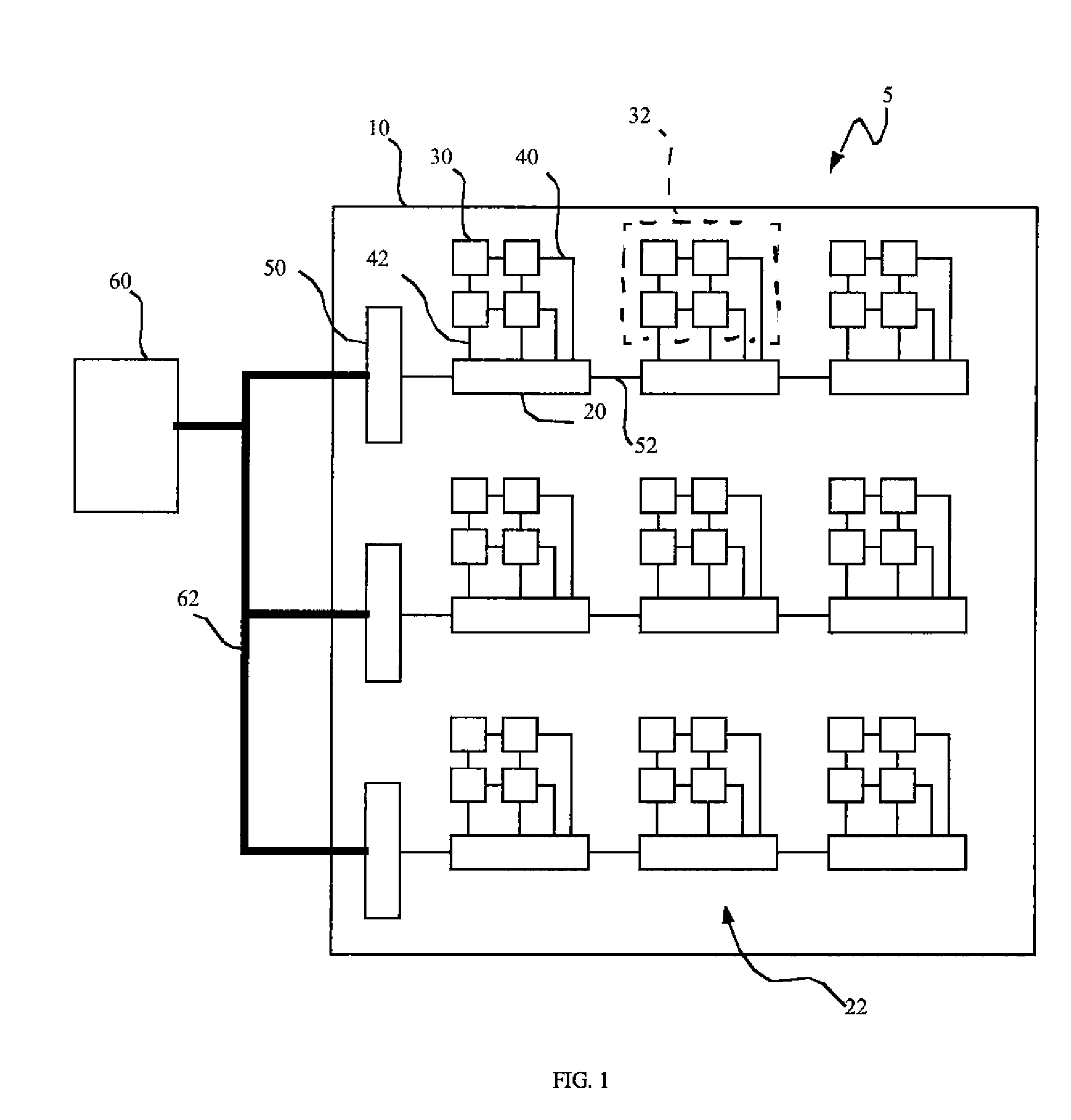
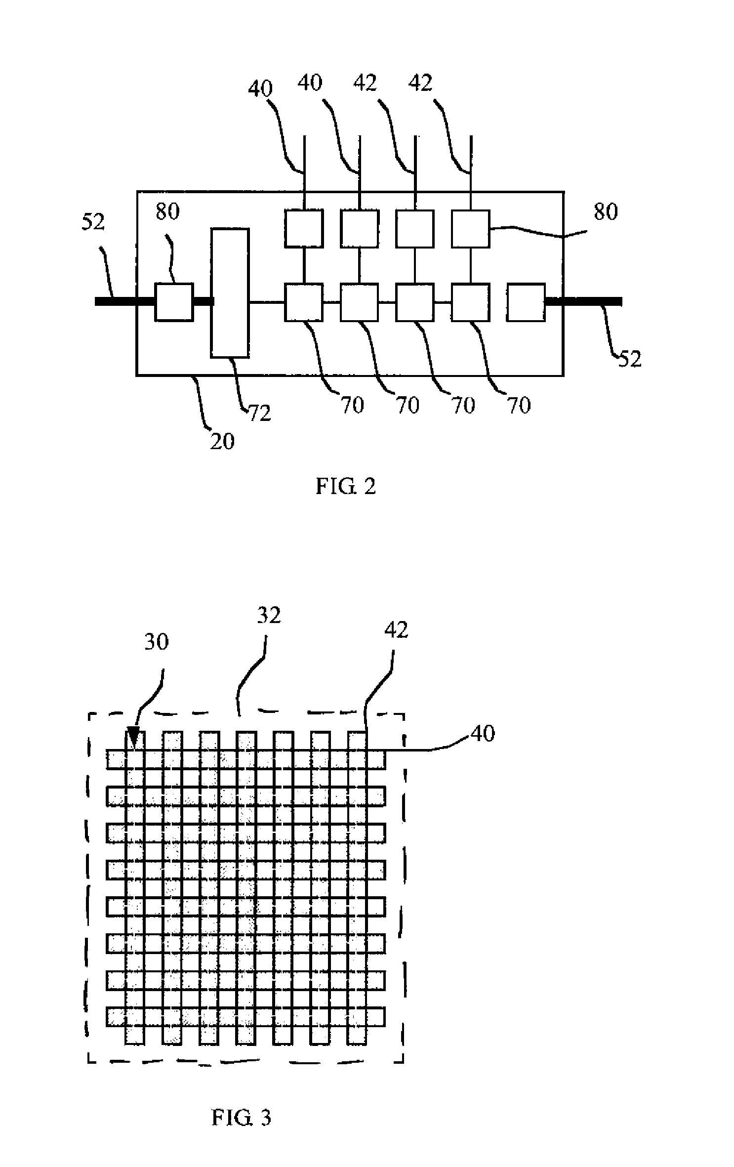
[0018]In one embodiment, the present invention comprises an imaging device having a hybrid drive. The imaging device can be, for example, an image display device (e.g. an emissive device) or an image capture device (e.g. a light-sensitive device). A hybrid drive, as disclosed herein, is a means for controlling the luminance of an array of light-emitting elements that combines attributes of both passive-matrix and active-matrix control. Referring to FIG. 1, the imaging device 5 comprises a single, continuous substrate 10. A two-dimensional pixel array is formed on the substrate 10, the pixels 30 associated into a plurality of pixel groups 32, each pixel group 32 including at least four pixels 30 and including a separate set of group row electrodes 40 and group column electrodes 42 connected to and driving only the pixels 30 in the corresponding pixel group 32, each of the group row electrodes 40 connected to two or more pixels 30 and each of the group column electrodes 42 connected t...


PUM


Abstract

A display device having a hybrid drive including a substrate, a two-dimensional pixel array formed on the substrate, the pixels associated into a plurality of pixel groups. A separate set of group row electrodes and group column electrodes are connected to pixels in pixel groups, so that a single group row electrode together with a single group column electrode drives a single pixel. Two or more chiplets are located over the substrate within the pixel array, each chiplet associated with a pixel group and having connections to each of the associated group row electrodes and associated group column electrodes and having storage elements, the storage element storing a value representing a desired luminance for a pixel and the chiplet using such value to control the desired luminance of each pixel in its associated pixel group.

Description

CROSS-REFERENCE TO RELATED APPLICATIONS[0001]The present application is related to U.S. application Ser. No. 12 / 191,462, filed Aug. 14, 2008, by Cok et al., and entitled, “Display Device With Chiplets.”FIELD OF THE INVENTION[0002]The present invention relates to display devices having a single, continuous substrate with distributed, independent control elements that provide a hybrid drive mechanism to an array of display pixel groups formed on the substrate.BACKGROUND OF THE INVENTION[0003]Flat-panel display devices are widely used in conjunction with computing devices, in portable devices, and for entertainment devices such as televisions. Such displays typically employ a plurality of pixels distributed over a substrate to display images. Each pixel incorporates several, differently colored light-emitting elements commonly referred to as sub-pixels, typically emitting red, green, and blue light, to represent each image element. As used herein, pixels can refer to a single light-emi...

Claims


Application Information

Patent Timeline
IPC IPC(8): G06F3/038
CPCG09G3/20G09G3/2085G09G3/2088H01L27/3281G09G2300/0426G09G2320/0247H01L27/3255G09G3/3225H10K59/129H10K59/17G09G3/36G09G3/32H10K59/00
Inventor COK, RONALD S.HAMER, JOHN W.VERES, JANOS
Owner GLOBAL OLED TECH
Why Eureka
Try Eureka