
Cavity-enhanced on-chip absorption spectroscopy

a technology of absorption spectroscopy and cavity enhancement, applied in the field of absorption spectroscopy, can solve the problems of destroying the advantage of being small, not reaching great efficiency of current spectroscopy devices using microresonators, and not realizing the full advantage of their small scal

Active Publication Date: 2010-05-20
CORNELL UNIVERSITY
View PDF21 Cites 20 Cited by
  • Summary
  • Abstract
  • Description
  • Claims
  • Application Information

AI Technical Summary

Benefits of technology

[0010]There is provided embodiments of an optofluidic device that can provide completely on-chip, label-free, massively parallel analysis of analytes. In one embodiment, the device enables measurement of the absorption spectrum of less than 2 nL of an analyte with resolutions possible at less than 1 nm and sensitivity equivalent to that of macroscopic systems.

Problems solved by technology

Current spectroscopy devices using microresonators have not reached great efficiency or realized the full advantage of their small scale.
Some devices defeat the advantage of being small by using some large scale components or requiring other components that could be eliminated.

Method used


Image

  • Cavity-enhanced on-chip absorption spectroscopy
  • Cavity-enhanced on-chip absorption spectroscopy
  • Cavity-enhanced on-chip absorption spectroscopy

Examples


Embodiment Construction

[0020]There is described an optofluidic absorption spectroscopy apparatus in which a range of input optical waveforms (i.e. input light) are subjected to an analyte and the absorption spectrum is measured and calculated. The input light couples with a microresonator. The light resonates through the microresonator, thereby increasing the optical path length, increasing the duration the light is exposed to the analyte, and increasing the resulting degree of sensitivity in measuring the absorption spectrum.

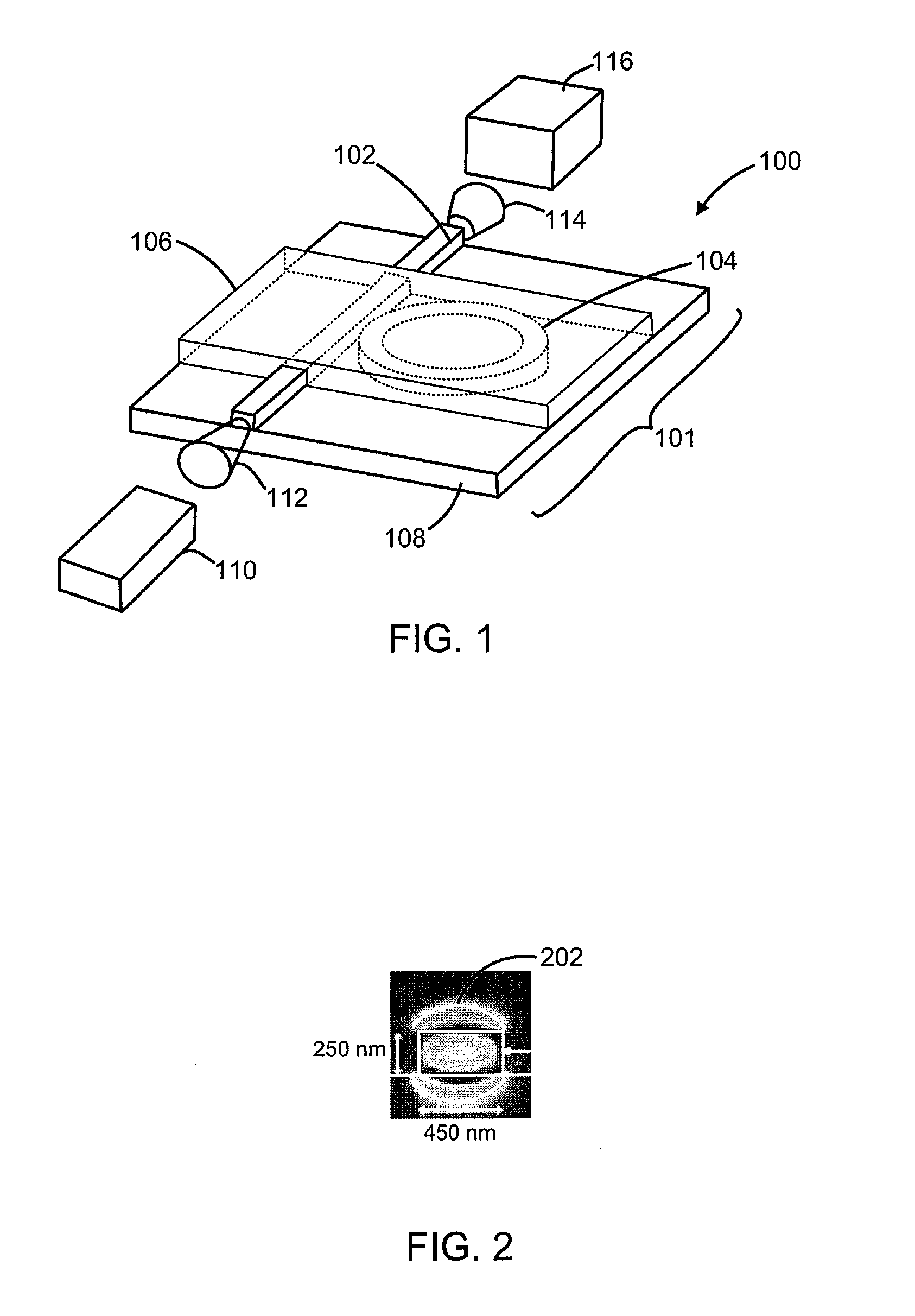
[0021]An example of an on-chip optofluidic absorption spectroscopy apparatus 100 according to the present description is shown in FIG. 1. The optofluidic absorption spectroscopy apparatus 100 can comprise an optofluidic portion 101, which can comprise a coupling waveguide 102, a resonator 104, a fluidic channel 106, and a base 108. Further, the absorption spectroscopy apparatus 100 can also comprise a light source 110, an input coupling lens 112, an output coupling lens 114, and a ph...


PUM


Abstract

Embodiments of optofluidic devices or methods according to the application can provide on-chip, label-free, massively parallel analysis of analytes. An embodiment of the optofluidic device can comprise a microresonator, a waveguide optically coupled to the microresonator, and a fluidic channel that exposes an analyte to an evanescent field from the microresonator, wherein the light signal has a linewidth lesser than the width of at least one resonance of the light signal propagating in the microresonator. The light signal can be tuned across a spectrum of light wavelengths, wherein the spectrum of wavelengths includes one or more wavelengths defining the at least one resonance in the microresonator. The light transmission through the waveguide over the spectrum of wavelengths of the input light can be detected, and an absorption spectrum of the analyte can be determined.

Description

CROSS REFERENCE TO RELATED APPLICATIONS[0001]This application claims benefit under U.S.C. 119(e) of U.S. Provisional Application No. 61 / 114,761, filed Nov. 14, 2008, entitled “Cavity-Enhanced On-Chip Absorption Spectroscopy”, which is incorporated herein by reference in its entirety.FIELD OF THE INVENTION[0002]The invention relates to absorption spectroscopy in general and specifically to miniature absorption spectroscopy systems for on-chip use in chemical analysis and biological analyte detection.BACKGROUND OF THE INVENTION[0003]Detection, identification, and analysis of analytes using absorption spectroscopy are known at a macroscopic scale. Such processes require light to interact with an examined analyte for a period of time easily achieved at macroscopic levels. Generally, a setup comprises a fixed length, single pass optical path through an analyte, in which some sort of light source inputs light through the optical path, and some sort of detector detects the light at the end...

Claims


Application Information

Patent Timeline
IPC IPC(8): G01N21/75G01N21/00
CPCG01N2021/7786G01N21/7746
Inventor NITKOWSKI, ARTHURLIPSON, MICHAL
Owner CORNELL UNIVERSITY
Learn More