
Semiconductor memory apparatus and test circuit therefor

a technology of semiconductor memory and test circuit, which is applied in the direction of information storage, static storage, digital storage, etc., can solve the problems of deterioration of repair efficiency and yield, deterioration of reliability of semiconductor memory apparatus, etc., and achieve the effect of improving repair efficiency

Active Publication Date: 2010-05-27
SK HYNIX INC
View PDF8 Cites 10 Cited by
  • Summary
  • Abstract
  • Description
  • Claims
  • Application Information

AI Technical Summary

Benefits of technology

[0013]Further, a semiconductor memory apparatus and a test circuit therefor that can improve repair efficiency in a semiconductor memory apparatus of an open bit-line structure are disclosed herein.

Problems solved by technology

However, when the repair is performed, the bit-line and the bit-line-bar are repaired independently from each other or only one of two is repaired, such that reliability of the semiconductor memory apparatus is deteriorated.
Therefore repair efficiency and yield are deteriorated.

Method used


Image

  • Semiconductor memory apparatus and test circuit therefor
  • Semiconductor memory apparatus and test circuit therefor
  • Semiconductor memory apparatus and test circuit therefor

Examples


Embodiment Construction

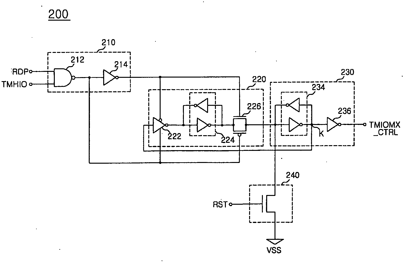
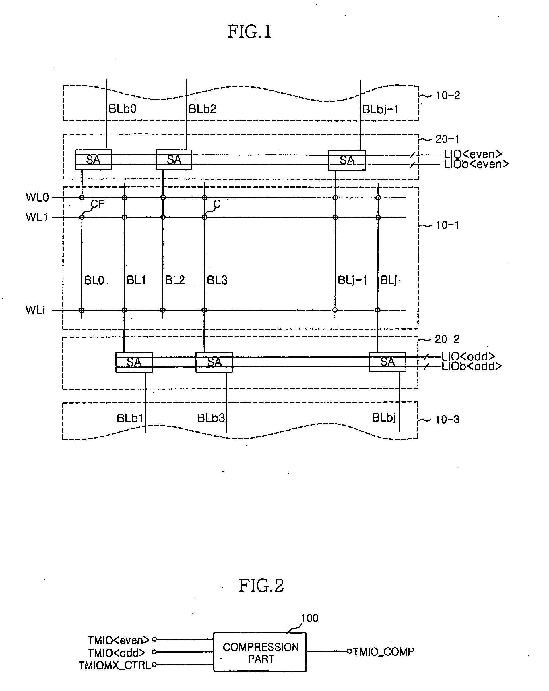
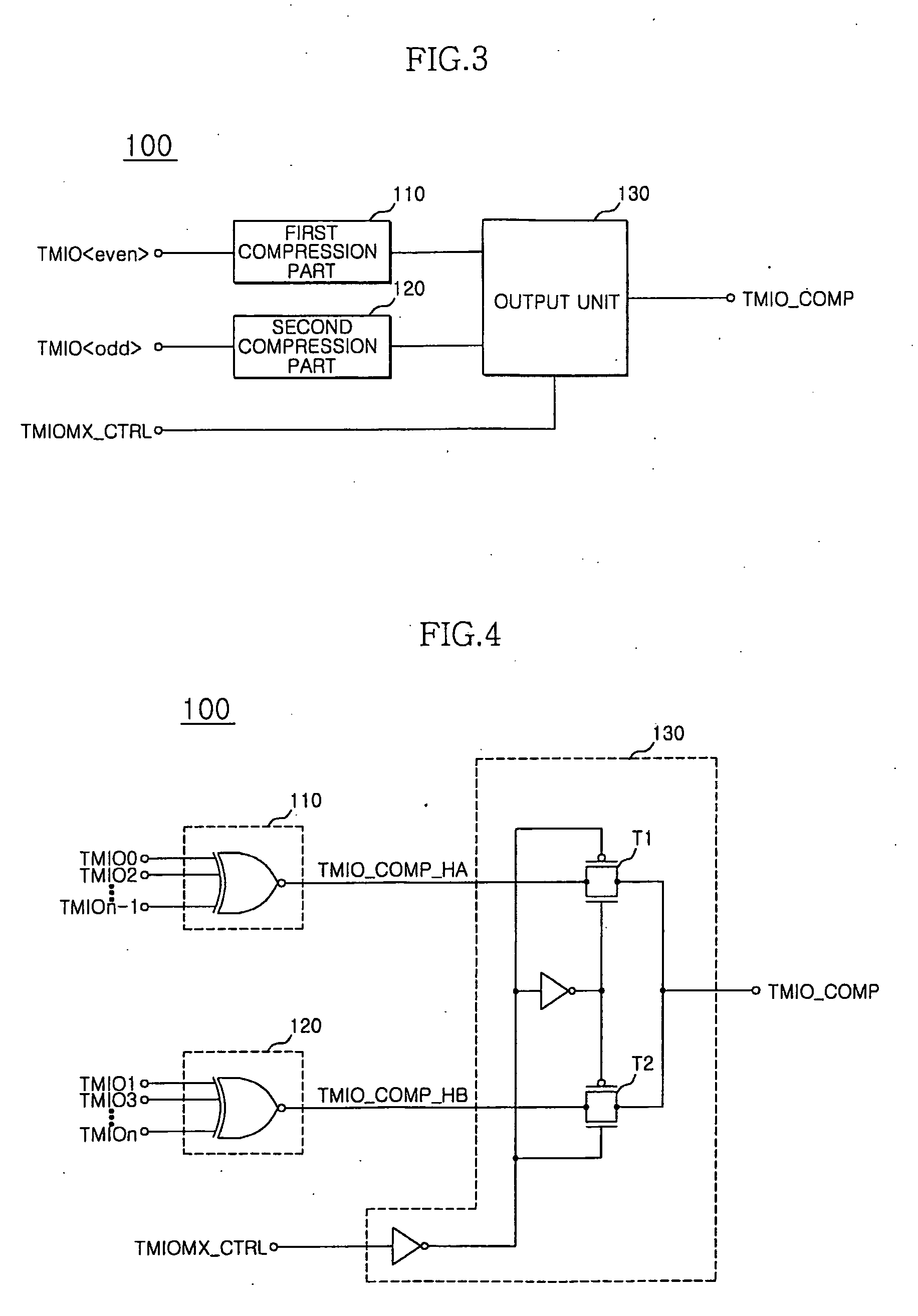
[0026]FIG. 2 is a configuration diagram of an exemplary test circuit of a semiconductor memory apparatus according to one embodiment.

[0027]As shown in the figure, the test circuit according to one embodiment can include a compression part 100 that can receive data (hereinafter, referred to as “test data”) ‘TMIO’ that are read from memory cells included in each cell mat and a compression control signal ‘TMIOMX_CTRL’ and output a compression test signal ‘TMIO_COMP’ by compressing test data ‘TMIO’ and ‘TMIO’ read from memory cells sharing a sense amplifier block, in a test mode of a semiconductor memory apparatus of an open bit-line structure.

[0028]More specifically, in the test mode, when word lines ‘WL0’ to ‘WLi’ of a first cell mat are selected and bit-lines ‘BL0’ to ‘BLj’ are activated, sense amplifiers ‘SA’ output data stored in each memory cell in accordance with a potential difference between the bit-line and the bit-line-bar through local input / output lines.

[0029]At this time, ...


PUM


Abstract

A test circuit for a semiconductor memory apparatus of an open bit-line structure includes a compression part configured to, in response to test data read from a plurality of memory cells included in a test target cell mat and a compression control signal generated from a compression control signal generating part, compress the test data that are read from the memory cells that share a sense amplifier block and sequentially output compression test signals.

Description

CROSS-REFERENCES TO RELATED PATENT APPLICATION[0001]The present application claims priority under 35 U.S.C 119(a) to Korean Application No. 10-2008-0118706, filed on Nov. 27, 2008, in the Korean Intellectual Property Office, which is incorporated herein by reference in its entirety as set forth herein in full.BACKGROUND[0002]1. Technical Field[0003]The embodiment described herein relates to a semiconductor memory apparatus and, more particularly, to a semiconductor memory apparatus and a test circuit therefor.[0004]2. Related Art[0005]In order to realize high integration of semiconductor memory apparatuses, the semiconductor memory apparatuses are being implemented in an open bit-line structure (6F2).[0006]Unlike known folded bit-line structures in which a bit-line and a bit-line-bar are provided in the same cell mat, the bit-line and the bit-line-bar are provided in different cell mats in open bit-line structures.[0007]FIG. 1 is a diagram for illustrating a structure of a known ope...

Claims


Application Information

Patent Timeline
IPC IPC(8): G11C7/00G11C29/00
CPCG11C29/40G11C29/44G11C2029/5602G11C29/56008G11C29/56G11C29/00G11C7/10
Inventor KIM, SEUNG BONG
Owner SK HYNIX INC
Learn More