
Integrated circuit packaging system with interposer and flip chip and method of manufacture thereof

Inactive Publication Date: 2010-06-03
STATS CHIPPAC LTD
View PDF13 Cites 31 Cited by
  • Summary
  • Abstract
  • Description
  • Claims
  • Application Information

AI Technical Summary

Problems solved by technology

Different challenges arise from increased functionality integration and miniaturization.
Further, increased performance of semiconductor product put additional challenges on the semiconductor product during test and in the field.
Solutions to these problems have been long sought but prior developments have not taught or suggested any solutions and, thus, solutions to these problems have long eluded those skilled in the art.

Method used


Image

  • Integrated circuit packaging system with interposer and flip chip and method of manufacture thereof
  • Integrated circuit packaging system with interposer and flip chip and method of manufacture thereof
  • Integrated circuit packaging system with interposer and flip chip and method of manufacture thereof

Examples


first embodiment

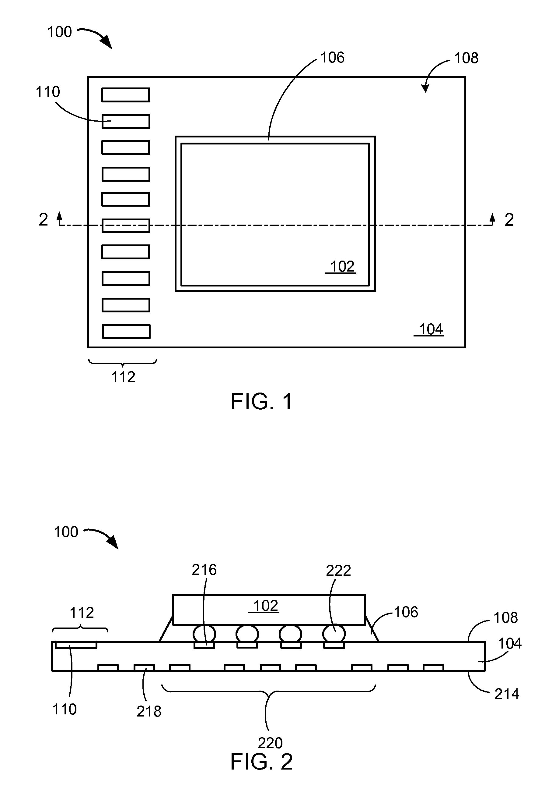
[0030]Referring now to FIG. 1, therein is shown a top view of an integrated circuit packaging system 100 in the present invention. The top view depicts an integrated circuit 102, such as a flip chip, mounted over an interposer 104, such as a laminated substrate, with an underfill 106 in between. The interposer 104 includes a first side 108 having a row of interconnect contacts 110 at a peripheral portion 112 of the interposer 104.

[0031]The interconnect contacts 110 are sized to provide surface areas for reliable connection. For example, the surface area of each of the interconnect contacts 110 are sufficient large for robust and reliable wire bonding onto the interconnect contacts 110.

[0032]For illustrative purposes, the integrated circuit packaging system 100 is shown with one row of the interconnect contacts 110, although it is understood that the integrated circuit packaging system 100 can have a different configuration with the interconnect contacts 110. For example, the integra...

second embodiment

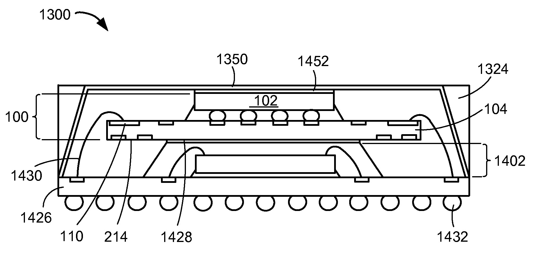
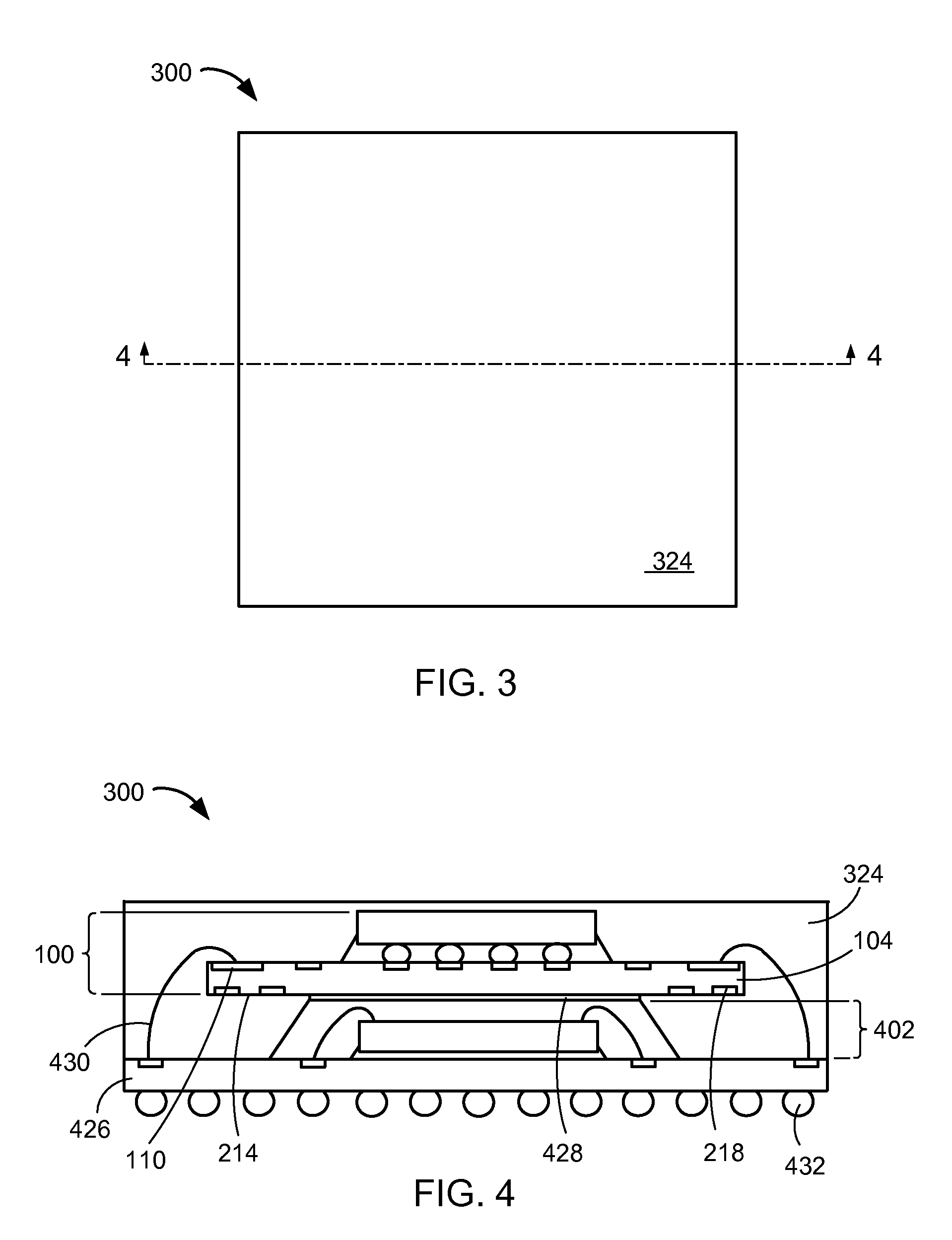
[0043]Referring now to FIG. 3, therein is shown a top view of an integrated circuit package-in-package system 300 in a first application example of the integrated circuit packaging system 100 of FIG. 1 in the present invention. The integrated circuit package-in-package system 300 includes a package encapsulation 324, such as a cover including an epoxy molding compound.

[0044]For illustrative purposes, the integrated circuit package-in-package system 300 is shown with a square geometric shape, although it is understood that the shape of the integrated circuit package-in-package system 300 may be different. For example, the integrated circuit package-in-package system 300 can have a rectangular shape.

[0045]Referring now to FIG. 4, therein is shown a cross-sectional view of the integrated circuit package-in-package system 300 along line 4-4 of FIG. 3. The cross-sectional view depicts the integrated circuit package-in-package system 300 having an integrated circuit device 402, such as an...

third embodiment

[0049]Referring now to FIG. 5, therein is shown a cross-sectional view of an integrated circuit package-in-package system 500 in a second application example of the integrated circuit packaging system 100 of FIG. 1 as exemplified by the top view of FIG. 3 in the present invention. The cross-sectional view depicts the integrated circuit package-in-package system 500 having an integrated circuit device 502, such as a flip chip, over a carrier 526, such as a laminated substrate.

[0050]An underfill support 534 can be between the integrated circuit device 502 and the carrier 526. The underfill support 534 can be same material as the underfill 106 of the integrated circuit packaging system 100. The underfill support 534 can surround and provide structural support to device interconnects 536, such as solder bumps or conductive bumps, of the integrated circuit device 502. The device interconnects 536 can connect the integrated circuit device 502 and the carrier 526.

[0051]The integrated circu...


PUM


Abstract

A method of manufacture of an integrated circuit packaging system includes: providing an interposer having a first side and a second side with the first side having a device contact and an interconnect contact and with the second side having a test pad; mounting an integrated circuit over the device contact; and applying an underfill between the integrated circuit and the interposer.

Description

TECHNICAL FIELD[0001]The present invention relates generally to an integrated circuit packaging system and more particularly to a system for an integrated circuit packaging system with an interposer.BACKGROUND ART[0002]Increased miniaturization of components, greater packaging density of integrated circuits (“ICs”), higher performance, and lower cost are ongoing goals of the computer industry. Semiconductor package structures continue to advance toward miniaturization, to increase the density of the components that are packaged therein while decreasing the sizes of the products that are made therefrom. This is in response to continually increasing demands on information and communication products for ever-reduced sizes, thicknesses, and costs, along with ever-increasing performance.[0003]These increasing requirements for miniaturization are particularly noteworthy, for example, in portable information and communication devices such as cellular phones, hands-free cellular phone heads...

Claims


Application Information

Patent Timeline
IPC IPC(8): H01L21/56H01L23/00
CPCH01L21/563H01L23/3128H01L2224/32225H01L24/48H01L2924/3025H01L2924/19107H01L2924/18161H01L2924/15311H01L2924/01079H01L2225/06572H01L2225/06517H01L2225/0651H01L2224/73265H01L2224/73253H01L2224/73204H01L2224/73203H01L2224/48227H01L2224/48225H01L2224/16225H01L23/552H01L25/0652H01L25/0657H01L2924/00012H01L24/73H01L2224/45014H01L2924/00014H01L2924/14H01L2924/181H01L2924/00H01L2224/45015H01L2924/207H01L2924/206
Inventor DO, BYUNG TAIPAGAILA, REZA ARGENTYCHUA, LINDA PEI EE
Owner STATS CHIPPAC LTD
Features
  • Generate Ideas
  • Intellectual Property
  • Life Sciences
  • Materials
  • Tech Scout
  • Unparalleled Data Quality
  • Higher Quality Content
  • 60% Fewer Hallucinations
Learn More