
Method of driving a gate line, gate drive circuit and display apparatus having the gate drive circuit

a gate drive circuit and display apparatus technology, applied in the field of gate drive circuits and display apparatuses, can solve the problems of abnormal gate on signal generation during gate off signal intervals, and achieve the effect of preventing ripples and substantially enhancing the reliability of the gate drive circuit outputing gate signals

Active Publication Date: 2010-06-03
SAMSUNG DISPLAY CO LTD
View PDF6 Cites 35 Cited by
  • Summary
  • Abstract
  • Description
  • Claims
  • Application Information

AI Technical Summary

Benefits of technology

[0010]Exemplary embodiments of the present invention provide a method of driving a gate line having substantially enhanced reliability of an operation thereof.
[0013]According to an exemplary embodiment of the present invention, a method of driving a gate line includes: charging one of a scan start signal and a carry signal provided from a previous stage to a first node of a present stage; outputting a gate signal through a gate node of the present stage by pulling-up a high level of a first clock signal at the first node to boost up a voltage potential of the first node; discharging the voltage potential of the first node and a voltage potential of the gate node to hold the first node and the gate node at a first power voltage as the first clock signal is shifted to a low level; and receiving a voltage potential signal of a second node of the previous stage, the second node holding a gate signal outputted from the previous stage, to reduce a ripple generated at the first node.
[0018]According to an alternative exemplary embodiment of the present invention, a gate drive circuit includes cascaded stages, the cascaded stages including a first stage to which a scan start signal is provided to an input terminal thereof. Each stage of the cascaded stages includes: a charging section which charges one of the scan start signal and a carry signal provided from a previous stage to a first node; a driving section connected to the charging section at the first node, the driving section configured to pull up a high level of a first clock signal to output a gate signal through a gate node as the first node is charged to a high level; a first discharging section which discharges a voltage potential of the first node and a voltage potential of the gate node to hold the voltage potential of the first node and the voltage potential of the gate node at a first power voltage as the first clock signal is shifted to a low level; and a second discharging section which receives a voltage potential signal of a second node of a previous stage, which holds a gate signal outputted from the previous stage, to reduce ripples generated at the first node.
[0019]In an exemplary embodiment of the present invention, the second discharging section may include a ripple-restraining transistor including a drain connected to the first power voltage, a source connected to the first node and a gate connected to the second node of the previous stage. The gate of the ripple-restraining transistor may maintain the first power voltage during a charging time of the first node to reduce ripples generated at the first node.
[0026]According to another alternative exemplary embodiment of the present invention, a display apparatus includes a display panel, a data drive circuit and a gate drive circuit. The display panel includes pixel parts connected to gate lines and data lines crossing the gate lines. The data drive circuit provides the data lines with a data voltage. The gate drive includes cascaded stages. Each of the cascaded stages includes a charging section, a driving section, a first discharging section and a second discharging section. The charging section charges a scan start signal or a carry signal provided from a previous stage to a first node. The driving section is connected to the charging section through the first node. The driving section pulls up a high level of a first clock signal to output a gate signal through a gate node as the first node is charged to a high level. The first discharging section discharges a voltage potential of the first node and a voltage potential of the gate node to hold the voltage potential of the first node and the voltage potential of the gate node to a first power voltage as the first clock signal is shifted to a low level. The second discharging section receives a voltage potential signal of a second node of a previous stage, which holds a gate signal outputted from the previous stage, to reduce ripple components generated at the first node.
[0031]Thus, in a method of driving a gate line, a gate drive circuit and a display apparatus having the gate drive circuit according to exemplary embodiments of the present invention, a gate of a transistor which discharges a first node at a present stage is connected to an output of a second node which is outputted from a previous stage to hold a gate signal. As a result ripples are effectively prevented from being generated during an interval period during which the gate signal is held at a first power voltage, and a reliability of an operation of the gate drive circuit which outputs a gate signal is substantially enhanced.

Problems solved by technology

However, when a gate drive circuit integrated on the display substrate is driven at a high temperature, noise from an abnormal gate on signal is generated during a gate off signal interval is generated.

Method used


Image

  • Method of driving a gate line, gate drive circuit and display apparatus having the gate drive circuit
  • Method of driving a gate line, gate drive circuit and display apparatus having the gate drive circuit
  • Method of driving a gate line, gate drive circuit and display apparatus having the gate drive circuit

Examples


Embodiment Construction

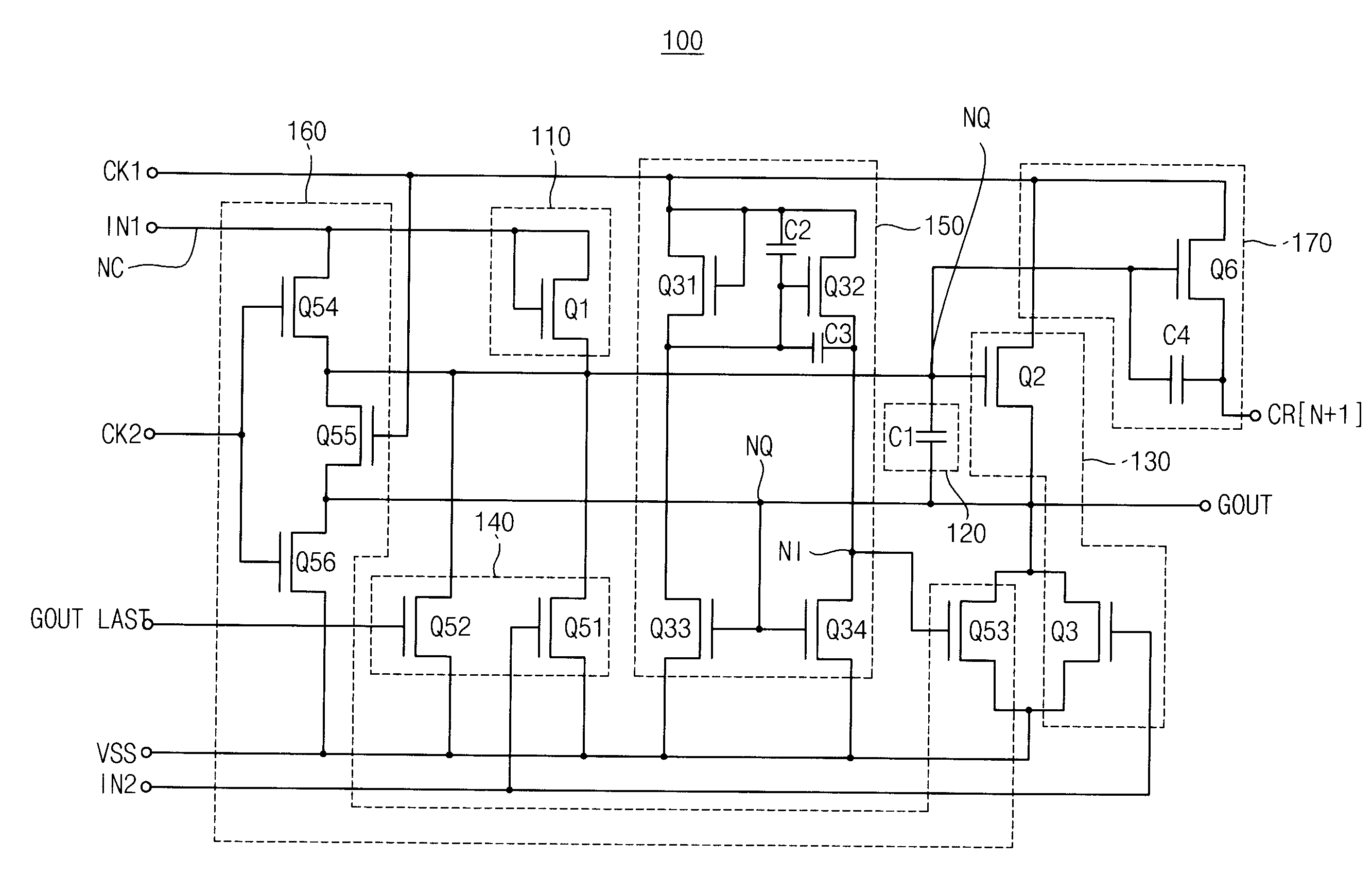
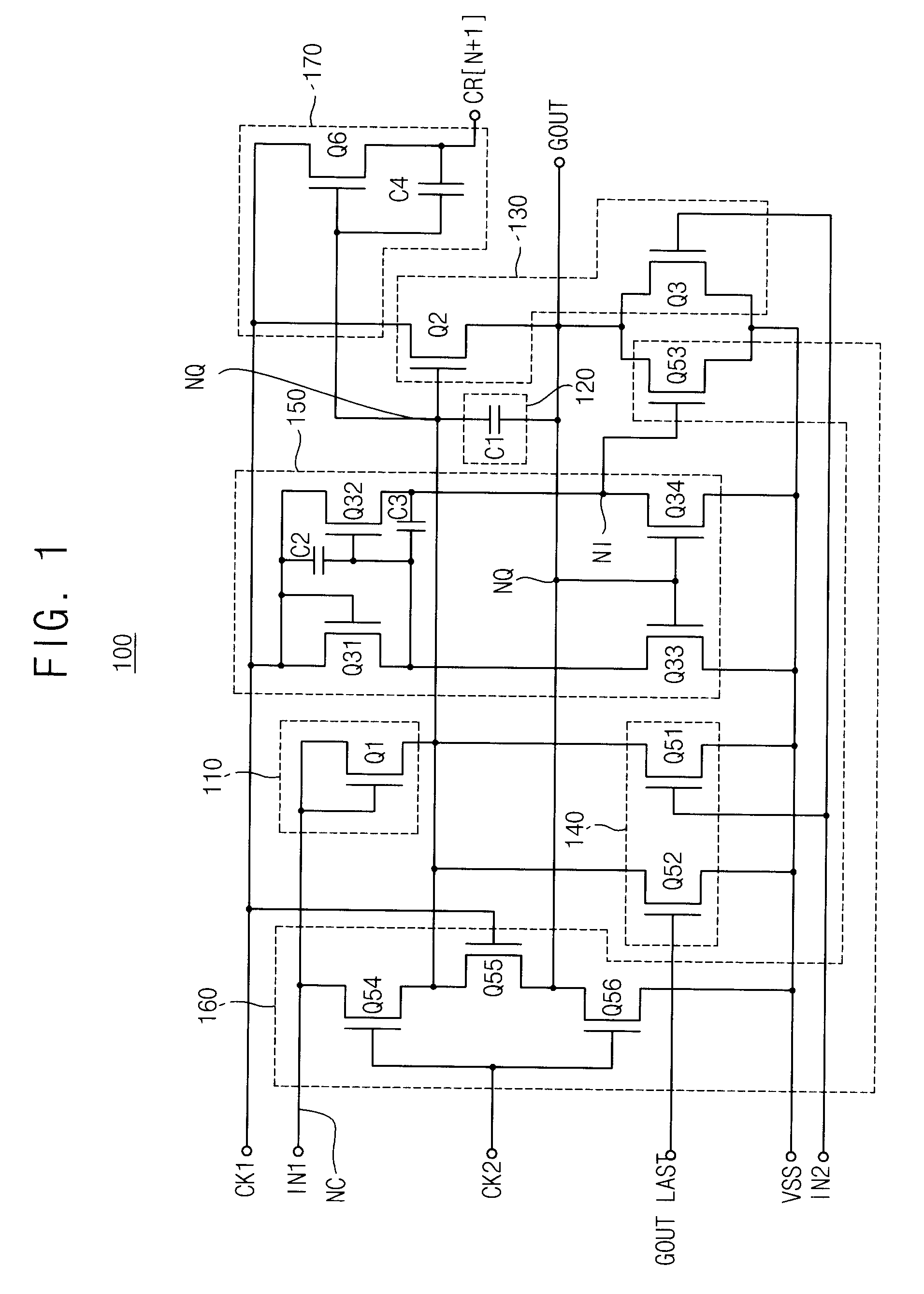
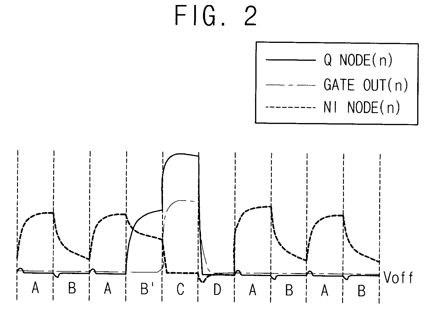
[0048]The invention will now be described more fully hereinafter with reference to the accompanying drawings, in which exemplary embodiments of the invention are shown. The present invention may, however, be embodied in many different forms and should not be construed as limited to the embodiments set forth herein. Rather, these embodiments are provided so that this disclosure will be thorough and complete, and will fully convey the scope of the invention to those skilled in the art. Like reference numerals refer to like elements throughout.

[0049]It will be understood that when an element is referred to as being “on” another element, it can be directly on the other element or intervening elements may be present therebetween. In contrast, when an element is referred to as being “directly on” another element, there are no intervening elements present. As used herein, the term “and / or” includes any and all combinations of one or more of the associated listed items.

[0050]It will be unde...


PUM


Abstract

A method of driving a gate line includes: charging one of a scan start signal and a carry signal provided from a previous stage to a first node of a present stage; outputting a gate signal through a gate node of the present stage by pulling up a high level of a first clock signal at the first node to boost up a voltage potential of the first node; discharging the voltage potential of the first node and a voltage potential of the gate node to hold the first node and the gate node at a first power voltage as the first clock signal is shifted to a low level; and receiving a voltage potential signal of a second node of the previous stage, the second node holding a gate signal outputted from the previous stage, to reduce a ripple generated at the first node.

Description

[0001]This application claims priority to Korean Patent Application No. 2008-120156, filed on Nov. 28, 2008, and all the benefits accruing therefrom under 35 U.S.C. § 119, the contents of which in its entirety are herein incorporated by reference.BACKGROUND OF THE INVENTION[0002]1. Field of the Invention[0003]The present invention relates to a method of driving a gate line, a gate drive circuit and a display apparatus having the gate drive circuit. More particularly, the present invention relates to a method of driving a gate line in which reliability of an operation thereof is substantially enhanced, a gate drive circuit performing the method and a display apparatus having the gate drive circuit.[0004]2. Description of the Related Art[0005]Generally, a liquid crystal display (“LCD”) apparatus includes an LCD panel which displays images by controlling a light-transmitting ratio of liquid crystal molecules provided with light from a backlight assembly disposed below the LCD panel.[00...

Claims


Application Information

Patent Timeline
IPC IPC(8): G09G3/36
CPCG09G3/3677G11C19/28G11C19/184G09G2310/0286G02F1/133G09G3/20G09G3/36
Inventor KI, DONG-HYEONKWON, HO-KYOONLEE, JU-HEENA, BYOUNG-SUN
Owner SAMSUNG DISPLAY CO LTD
Learn More