Method for fabricating a nanostructured substrate for OLED and method for fabricating an OLED

a nanostructured substrate and oled technology, applied in the direction of electrical equipment, semiconductor devices, organic semiconductor devices, etc., can solve the problems of unusable oled stacks, serious difficulties in surviving subsequent treatment, and emitting molecules of these layers have serious problems, and achieve accurate adjustment of extraction and excess slope

Inactive Publication Date: 2010-06-03
COMMISSARIAT A LENERGIE ATOMIQUE ET AUX ENERGIES ALTERNATIVES
View PDF14 Cites 11 Cited by
  • Summary
  • Abstract
  • Description
  • Claims
  • Application Information

AI Technical Summary

Benefits of technology

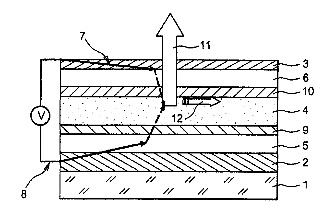
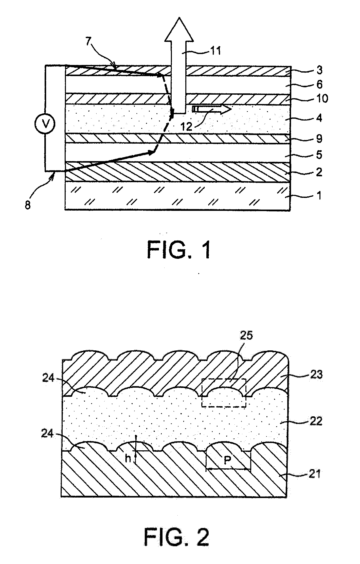
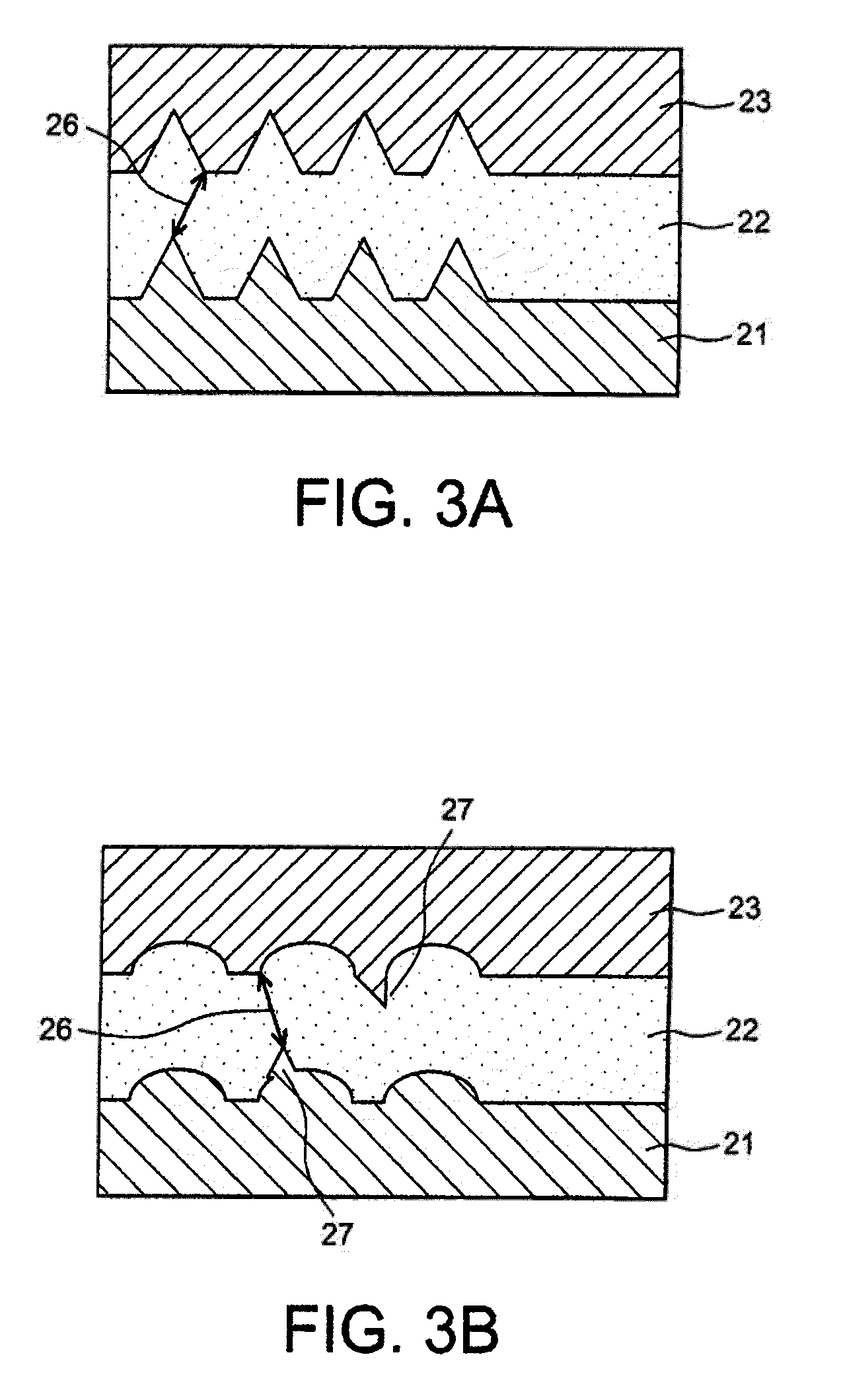
[0104]Thanks to the inventive method, substrates are obtained without local defects, without surface roughness, and the nanostructuration and particularly the shape of the patterns is perfectly and simply controlled by very simply adjusting the flow time, or annealing or relaxation time. The presence of patterns which are for example too “sharp” or have an excessive slope, is also avoided. In consequence, the nanostructuration and particularly the shape of the patterns of the layers subsequently deposited on the nanostructured surface is also controlled, and these layers no longer have defects, roughness or undesirable geometry. The shape of the patterns making up the extraction arrays of the diode is perfectly controlled and a reinforced but also accurately adjustable extraction can be obtained. Short-circuits in the diode prepared on the substrate prepared by the inventive method are also avoided.

Problems solved by technology

In all cases, these photons do not participate in the “useful light” of the diode.
However, a poorly controlled structuration can cause a short-circuiting of the two electrodes, making the OLED stack unusable.
Experience shows that the emitting molecules of these layers have serious difficulty withstanding the subsequent (“a posteriori”) treatments after the overall production of the diode.
Furthermore, both in the case of the nano-imprint technique and in the case of the other techniques for preparing substrates with a nanostructured surface, the control of the shape of the pattern is crucial, and may prove critical, because this shape has repercussions on all the layers which are then deposited to match this surface and therefore on the functioning of the overall device finally fabricated on this substrate such as an OLED.

Method used


Image

  • Method for fabricating a nanostructured substrate for OLED and method for fabricating an OLED
  • Method for fabricating a nanostructured substrate for OLED and method for fabricating an OLED
  • Method for fabricating a nanostructured substrate for OLED and method for fabricating an OLED

Examples


example 1

[0233]In this example, a substrate is prepared by the inventive method using a thermosetting resin, and an organic light emitting diode is then prepared on the said substrate by the inventive method.

[0234]The substrate preparation method comprises the following successive steps:[0235]deposition of the thermosetting resin Neb® 22 from Sumitomo Chemical Japan available on the market, on an 8 inch silicon wafer;[0236]compression of the resin at 110° C. for 5 minutes under 300 mbar, whereby a first nanostructuration is obtained, which is an array of lines or an array of bumps with a period of 200 to 600 nm and heights of 5 to 40 nm;[0237]flow at 125° C. for 60 seconds;[0238]solidification for example for 248 minutes at ambient temperature, and annealing at 90° C. for 60 seconds.

[0239]A second nanostructuration is thereby obtained, “flowed” and stable up to 200° C. which is an array of lines or an array of bumps with a period of 200 to 600 nm and heights of 5 to 40 nm.

[0240]The “OLED” la...

example 2

[0241]In this example, a substrate is prepared by the inventive method using a polystyrene resin, and an organic light emitting diode is then prepared on the said substrate by the inventive method.

[0242]The substrate preparation method comprises the following successive steps:[0243]deposition of the polystyrene resin, on an 8 inch silicon wafer;[0244]compression of the resin at 120° C. for 5 minutes under 300 mbar, whereby a first nanostructuration is obtained, which is an array of lines with a height of 35 nm and a period of 500 nm;[0245]flowing is carried out at a temperature of 150° C. for variable times;[0246]and solidification for example for 248 minutes at ambient temperature, and an annealing at 90° C. for 60 seconds is carried out.

[0247]The annealing or reflowing profiles obtained are then observed for the various flow times. The profiles are shown on the graph in FIG. 5.

[0248]Curve A (points □) shows the profile of the second nanostructuration for a flowing, “remelting” tim...


PUM

PropertyMeasurementUnit
melting pointaaaaaaaaaa
thicknessaaaaaaaaaa
thicknessaaaaaaaaaa

Abstract

Method for fabricating a substrate comprising a nanostructured surface for an organic light emitting diode OLED, in which a layer of an organic resin or of a mineral material having a first nanostructuration is prepared by nano-imprint; the organic resin or mineral material is heated to a temperature equal to or higher than its glass transition temperature Tg or its melting point, and the organic resin or the mineral material is maintained at this temperature for a time tR called annealing time, whereby the organic resin or the mineral material flows and the first nanostructuration of the layer of organic resin or of mineral material is modified to produce a second nanostructuration; the organic resin or the mineral material is cooled.

Description

CROSS REFERENCE TO RELATED APPLICATIONS OR PRIORITY CLAIM[0001]This application claims priority of French Patent Application No. 08 58120, filed Nov. 28, 2008.DESCRIPTION[0002]1. Technical Field[0003]The invention relates to a method for fabricating a substrate comprising a nanostructured surface for an organic light emitting diode OLED.[0004]The invention further relates to a method for fabricating an organic light emitting diode OLED comprising a step for fabricating a substrate comprising a nanostructured surface by the above method.[0005]The technical field of the invention can be defined as that of organic light emitting diodes and more particularly as that of organic light emitting diodes provided with nanostructurations for reinforcing the light extraction.[0006]2. Prior Art[0007]Organic light emitting diodes are new-generation diodes and constitute a highly promising technology for displays, such as television screens and computer screens, etc., and for lighting, thanks to t...

Claims


Application Information

Patent Timeline
Patent Type & Authority Applications(United States)
IPC IPC(8): H01L21/00
CPCH01L51/0001H01L2251/105H01L51/5275H01L51/5262H10K71/00H10K50/85H10K50/858H10K71/821
Inventor MARY, ALEXANDREANDRE, LUCLANDIS, STEFAN
Owner COMMISSARIAT A LENERGIE ATOMIQUE ET AUX ENERGIES ALTERNATIVES
Why Eureka
Try Eureka