Source Driver and Display Device Having the Same

Active Publication Date: 2010-06-10
SAMSUNG ELECTRONICS CO LTD
View PDF5 Cites 6 Cited by
  • Summary
  • Abstract
  • Description
  • Claims
  • Application Information

AI Technical Summary

Benefits of technology

[0008]The present general inventive concept provides a source driver capable of minimizing an error of voltage charged in each pixel and capable of charging each pixel with a voltage corresponding to a write data accurately, and a display device having the same.

Problems solved by technology

However, when the transistor is embodied as an amorphous silicon TFT (thin-film transistor), the capacitor Cps of a pixel may not be charged with a target voltage while a voltage is supplied since an on-resistor of the transistor is very great.

Method used


Image

  • Source Driver and Display Device Having the Same
  • Source Driver and Display Device Having the Same
  • Source Driver and Display Device Having the Same

Examples


Embodiment Construction

[0019]Reference will now be made in detail to exemplary embodiments of the present general inventive concept and the accompanying drawings, wherein like reference numerals may refer to the like elements throughout.

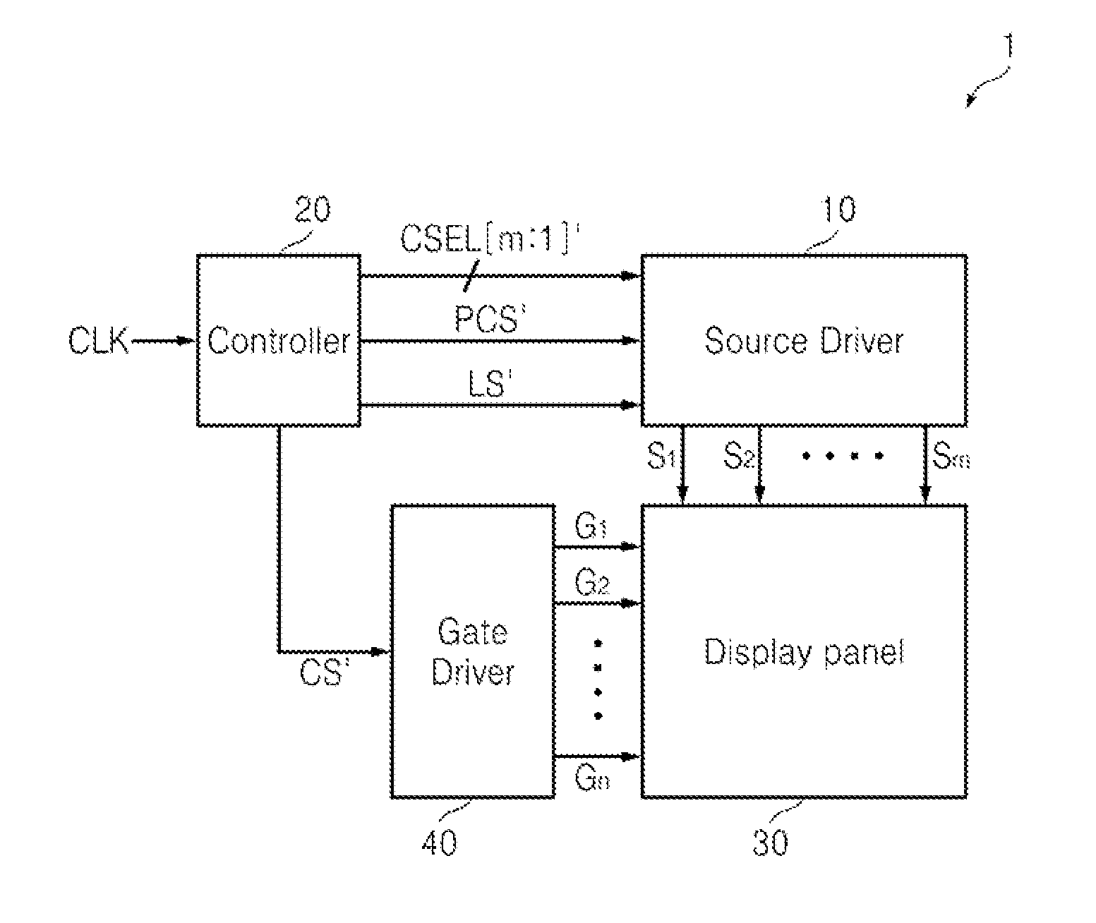
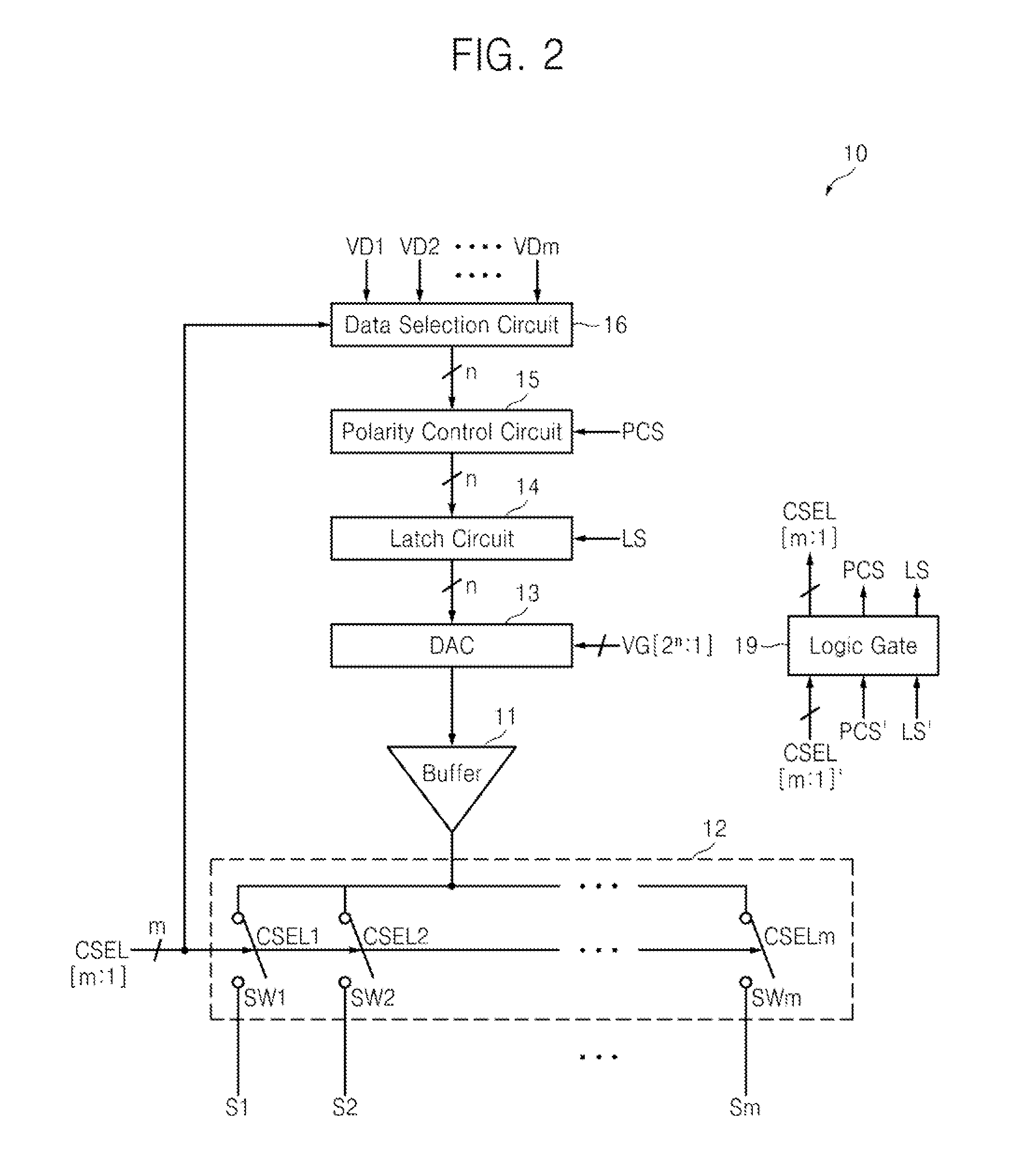
[0020]FIG. 2 is a block diagram of a source driver 10 according to an exemplary embodiment of the present invention. Referring to FIGS. 1 and 2, the source driver 10 may include a buffer 11 and a switching circuit 12. The buffer 11 may buffer a plurality of analog voltages corresponding to each of a plurality of digital image data VD1, VD2, . . . , VDm.

[0021]The switching circuit 12 may include a plurality of switches SW1 to SWm, where m is a positive integer. The plurality of switches SW1 to SWm are connected to an output terminal of the buffer 11 and a corresponding data line among a plurality of data lines S1, S2, . . . , Sm. The analog voltages may be supplied to each data line multiple times in response to a plurality of channel select signals CSEL[m:1] in a horizonta...


PUM


Abstract

A source driver and a display device having the same are provided. The source driver shares several outputs by using a time division method and has an analog voltage stored in a buffer supplied to each data line multiple times during a horizontal scanning interval. Accordingly, by supplying an analog voltage to a data line a first time in a first activation interval and supplying an analog voltage to a data line a second time in a second activation interval, a target voltage of each pixel may be achieved quickly and accurately.

Description

CROSS-REFERENCE TO RELATED APPLICATION[0001]This application claims priority under 35 U.S.C. §119 to Korean Patent Application No. 10-2008-0123252, filed on 5 Dec. 2008, in the Korean Intellectual Property Office, the disclosure of which is incorporated herein in its entirety by reference.BACKGROUND[0002]1. Technical Field[0003]The present invention relates to a display device, and more particularly, to a source driver and a display device having the same.[0004]2. Discussion of the Related Art[0005]A source driver called a data line driver converts a digital signal corresponding to image data into an analog voltage and displays the image data by supplying the converted analog voltage to each pixel of a display panel.[0006]FIG. 1 is a schematic diagram illustrating a display panel and an equivalent circuit of each pixel thereof. The display panel includes a plurality of data lines Si, Si+1, Si+2 and Si+3, a plurality of gate lines, Gj, Gj+1 and Gj+2, and a plurality of pixels formed ...

Claims


Application Information

Patent Timeline
Patent Type & Authority Applications(United States)
IPC IPC(8): G06F3/038
CPCG09G3/3685G09G3/2022G09G2310/0202G09G2330/023G09G2310/0297G09G2320/0223G09G2310/0291G02F1/133G09G3/20G09G3/36
Inventor BAEK, JONG HAKCHOI, YOON KYUNGKWON, OH-KYONG
Owner SAMSUNG ELECTRONICS CO LTD
Why Eureka
Try Eureka