Substrate processing apparatus and method of manufacturing semiconductor device

Active Publication Date: 2010-06-10
KOKUSA ELECTRIC CO LTD
View PDF8 Cites 12 Cited by
  • Summary
  • Abstract
  • Description
  • Claims
  • Application Information

AI Technical Summary

Benefits of technology

[0008]An object of the present invention is to provide a substrate processing apparatus capable of rap

Problems solved by technology

When a substrate processing process is performed, due to defects or malfunctioning of a substrate processing apparatus, steps of the substrate processing process can be delayed.
However, in case of a conventional substrate processing apparatus, it is difficult to enable an operator to perceive a delay of a process

Method used


Image

  • Substrate processing apparatus and method of manufacturing semiconductor device
  • Substrate processing apparatus and method of manufacturing semiconductor device
  • Substrate processing apparatus and method of manufacturing semiconductor device

Examples


embodiment 1

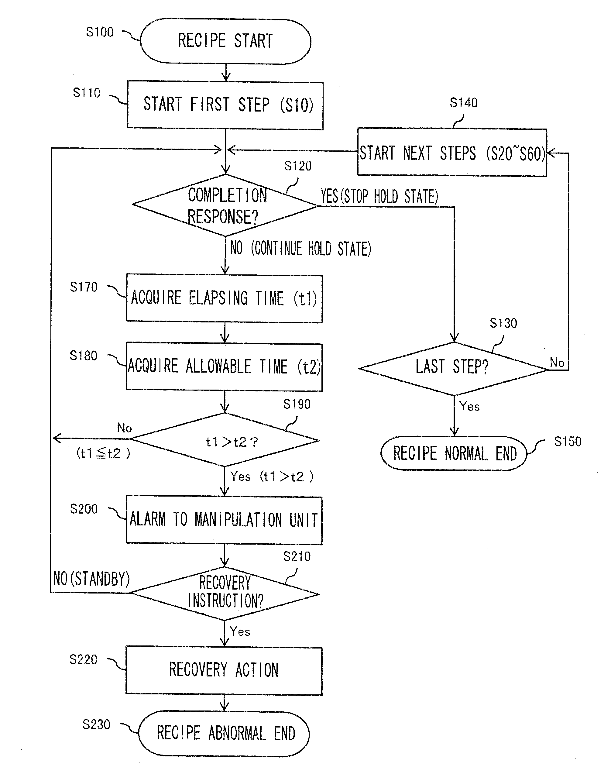
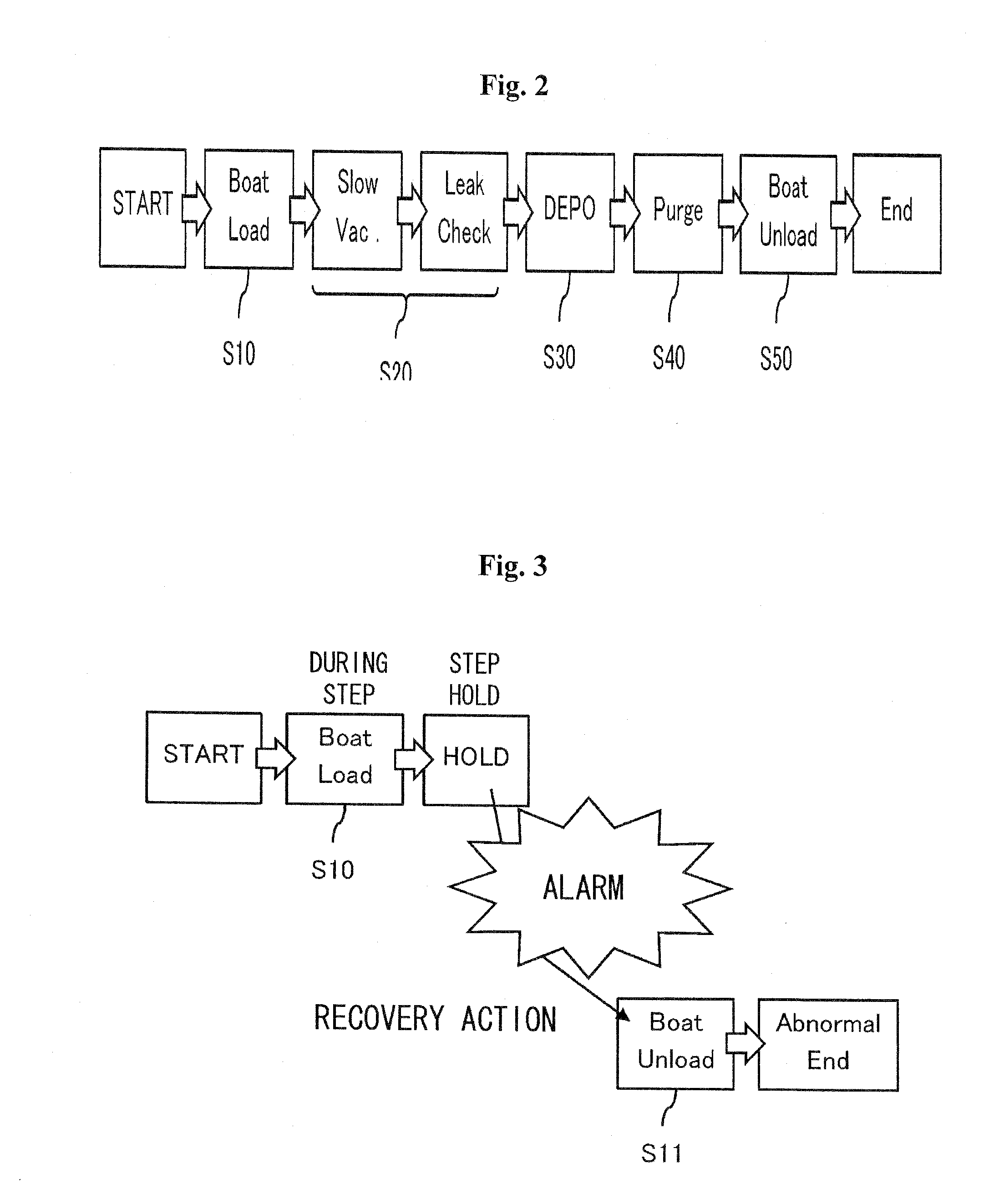
[0091]FIG. 3 is a flowchart for explaining an exemplary operation of the substrate processing apparatus in the case where the elapsing time of the boat load step S10 exceeds the allowable time.

[0092]Referring to FIG. 3, if the boat load step S10 is delayed, the control unit 3 staying in hold state writes an alarm message in a shared memory region to report that an elapsing time t1 exceeds an allowable time t2 so that the manipulation unit 2 can be informed of the delay of the boat load step S10 caused by a certain reason. Then, the control unit 3 staying in hold state reads an ┌error handling action (alarm condition table)┘ instruction from the shared memory region and perform a predetermined recovery action (boat unload step S11 in the current embodiment). If the control unit 3 receives a response reporting completion of the recovery action from a sub controller, the control unit 3 writes a message in the shared memory region to report an abnormal end of a recipe, and concurrently,...

embodiment 2

[0094]FIG. 4 is a flowchart for explaining another exemplary operation of the substrate processing apparatus in the case where the elapsing time of the boat load step S10 exceeds the allowable time.

[0095]Referring to FIG. 4, if the boat load step S10 is delayed, the control unit 3 staying in hold state writes an alarm message in a shared memory region to report that an elapsing time t1 exceeds an allowable time t2 so that the manipulation unit 2 can be informed of the delay of the boat load step S10 caused by a certain reason. Then, the control unit 3 staying in hold state reads an ┌error handling action (alarm condition table)┘ instruction from the shared memory region and perform a predetermined recovery action. In the current embodiment, a boat load step is performed again (S12), and then, the decompression (slow vac. and leak check) step S20, the film forming (DEPO) step S30, the atmospheric pressure return (purge) step S40, and the boat unload step S50 are sequentially performe...

embodiment 3

[0097]FIG. 5 is a flowchart for explaining an exemplary operation of the substrate processing apparatus in the case where the elapsing time of the compression (slow vac. and leak check) step S20 exceeds the allowable time.

[0098]Referring to FIG. 5, if the compression (slow vac. and leak check) step S20 is delayed (for example, if leak checking is unclear although exhausting (slow vac.) is retried a plurality of times), the control unit 3 staying in hold state writes an alarm message in a shared memory region to report that an elapsing time t1 exceeds an allowable time t2 so that the manipulation unit 2 can be informed of the delay of the compression (slow vac. and leak check) step S20 caused by a certain reason. Then, the control unit 3 staying in hold state reads an ┌error handling action (alarm condition table)┘ instruction from the shared memory region and perform a predetermined recovery action (an atmospheric pressure return (purge) step S21 and a boat unload step S22 in the cu...


PUM

PropertyMeasurementUnit
Timeaaaaaaaaaa

Abstract

When a step is delayed, an operator can be rapidly informed of the delay. A substrate processing apparatus comprises a process system configured to process a substrate, a control unit configured to control the process system for performing a plurality of steps, and a manipulation unit configured to monitor progresses of the steps. While the control unit waits for completion of a predetermined one of the steps after the control unit controls the process system to start the predetermined step, if a time elapsing from the start of the predetermined step exceeds an allowable time previously allocated to each of the steps, the control unit transmits an alarm message to the manipulation unit so as to report that the allowable time is exceeded.

Description

CROSS-REFERENCE TO RELATED PATENT APPLICATION[0001]This U.S. non-provisional patent application claims priority under 35 U.S.C. §119 of Japanese Patent Application No. 2008-313854, filed on Dec. 10, 2008, in the Japanese Patent Office, the entire contents of which are hereby incorporated by reference.BACKGROUND OF THE INVENTION[0002]1. Field of the Invention[0003]The present invention relates to a substrate processing apparatus configured to perform a plurality of steps sequentially and a method of manufacturing a semiconductor device.[0004]2. Description of the Prior Art[0005]As one of processes included in a method of manufacturing a semiconductor device such as an integrated circuit (IC) or dynamic random access memory (DRAM), there is a substrate processing process which includes sequential steps such as: a step of loading a substrate into a process furnace; a step of increasing the inside temperature of the process furnace to a film-forming temperature; a step of processing the...

Claims


Application Information

Patent Timeline
IPC IPC(8): H01L21/203B05C11/00
CPCC23C16/52C23C16/54G05B19/4063H01L21/67276G05B2219/31437G05B2219/45031G05B19/41875Y02P90/02G05B23/0205H01L21/0273H01L21/203H01L21/31
Inventor TAKAHATA, SATORUOZAKI, YUKIONUNOZAWA, REIZO
Owner KOKUSA ELECTRIC CO LTD
Why Eureka
Try Eureka