
Silicon germanium heterojunction bipolar transistor structure and method

a technology of silicon germanium and heterojunction, applied in the field of silicon germanium heterojunction bipolar transistors, can solve the problems of limited scaling, device scaling, and current process technology cannot make such a sic pedestal narrow, and achieve the effect of keeping the first dopant profile narrow and minimizing unwanted defect-enhanced diffusion

Inactive Publication Date: 2010-06-24
VEECO INSTR
View PDF16 Cites 4 Cited by
  • Summary
  • Abstract
  • Description
  • Claims
  • Application Information

AI Technical Summary

Benefits of technology

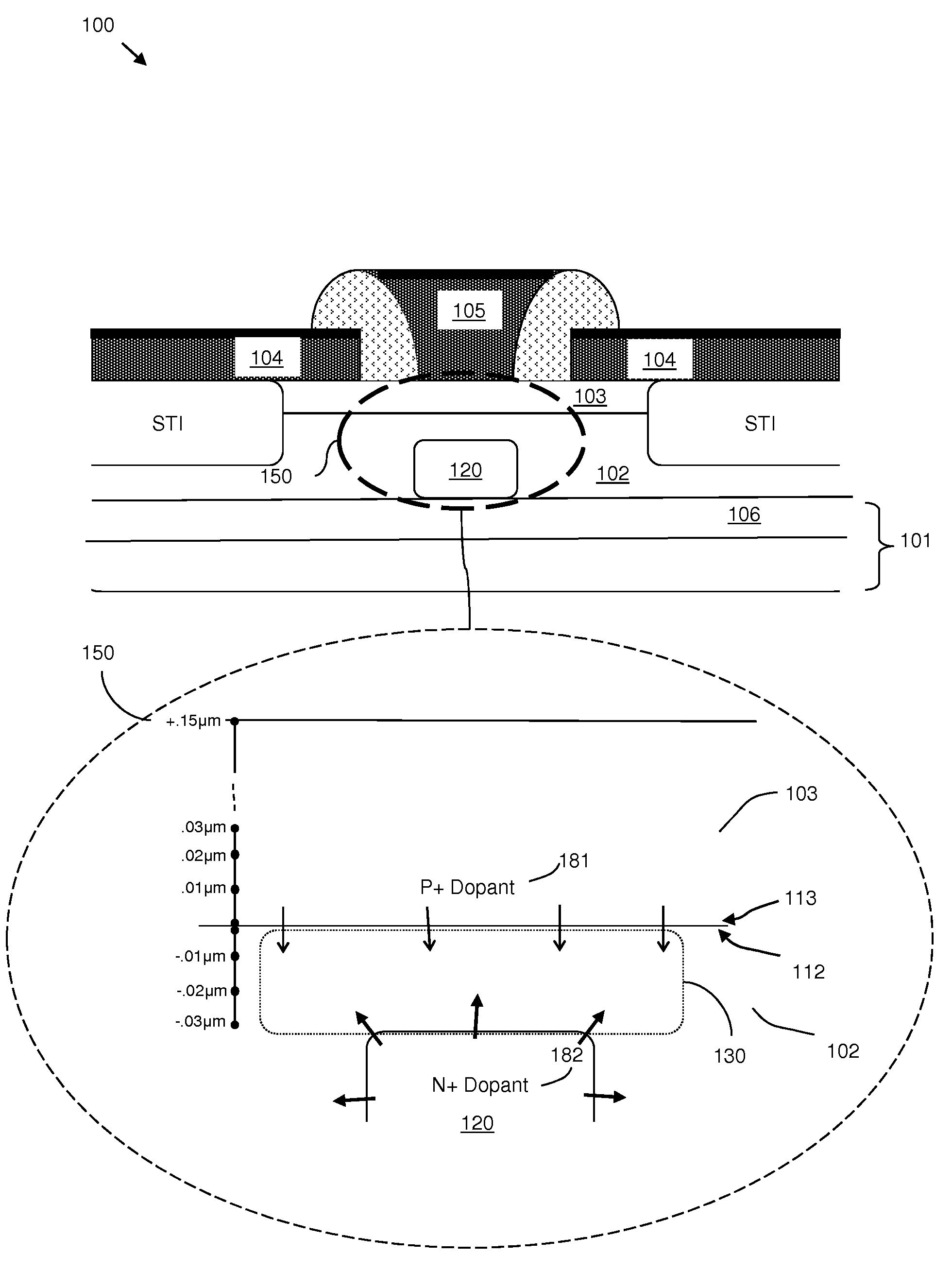
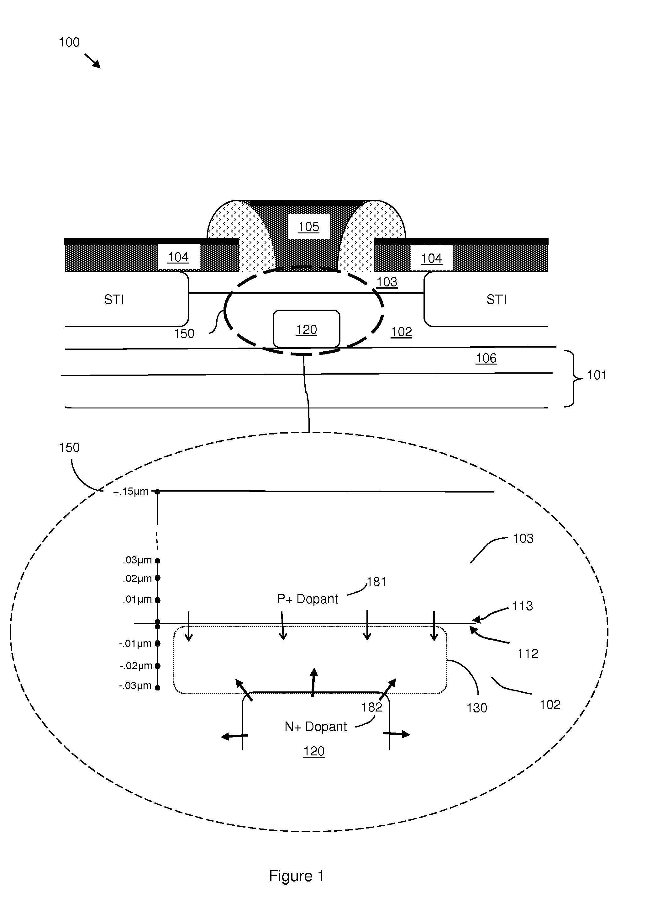
[0010]Thus, the diffusion region can comprise a portion of the first dopant diffused from the first semiconductor layer above and a portion of the second dopant diffused in from the implant region below. However, during the formation process, a laser anneal process can be performed to activate the dopants in the implant region and to remove defects (i.e., interstitials) from the top surface of the second semiconductor layer caused by the ion-implantation process that forms the implant region. Using a laser anneal process, vice a rapid thermal anneal process, minimizes diffusion of the second dopant from the implant region. Furthermore, since the top surface of the second semiconductor layer has approximately no defects, diffusion of the first dopant into the diffusion region from the first semiconductor layer into the second semiconductor layer is minimized.
[0014]Thus, the diffusion region can comprise a portion of the first dopant diffused from the base layer above and a portion of the second dopant diffused in from the implant region below. However, during the formation process, a laser anneal process can be performed to activate the dopants in the implant region and to remove defects from the top surface of the collector layer caused by the ion-implantation process that forms the implant region. Using a laser anneal process, vice a rapid thermal anneal process, minimizes diffusion of the second dopant from the implant region. Furthermore, since the top surface of the collector layer has approximately no defects, diffusion of the first dopant from the base layer into the collector layer below is minimized.
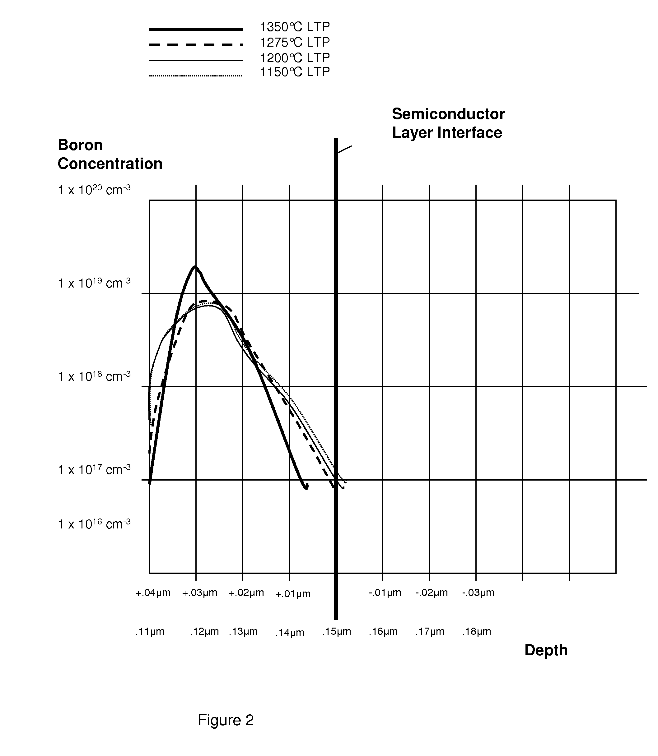
[0020]Following the implantation process, the second dopant in the implant region is activated and any defects that were formed on the top surface of the initial semiconductor layer as a result of the implantation process are removed by performing a laser anneal (e.g., a laser thermal process (LTP) or a laser spike anneal (LSA)). This laser anneal is performed at temperatures greater than approximately 1100° C. and using a technique that avoids melting of the initial semiconductor layer and achieves a thermal equilibrium in the semiconductor layer in less than approximately 10 ps (i.e., using a millisecond laser anneal process) in order to minimize diffusion of the second dopant from the implant region and, thereby, keep the second dopant profile narrow. Specifically, diffusion of the second dopant is minimized using this laser anneal such that a concentration profile of the second dopant outside of the implant region decreases (e.g., from approximately 1×1018 cm−3 at approximately 0.02 μm below the top surface of the initial semiconductor layer to less than approximately 1×1017 cm−3 near the top surface). The use of such a laser anneal further avoids clustering of point defects and forming of extended defects and dislocation loops at the top surface the semiconductor layer during subsequent processing. This LTP process methodology does not affect the impact of subsequent process conditions.
[0022]Diffusion of this first dopant from the additional semiconductor layer into the initial semiconductor layer below is minimized due to the defect removal process (discussed above). That is, removal of the defects at the top surface of the initial semiconductor layer by laser anneal minimizes unwanted defect-enhanced diffusion of the first dopant and, thereby, keeps the first dopant profile narrow. Specifically, diffusion of the first dopant from the additional semiconductor layer into the initial semiconductor layer below is minimized by the lack of defects at the interface (i.e., interstitials) such that a peak concentration of the first dopant in the additional semiconductor layer adjacent to the bottom surface can be at least 100 times or greater than the concentration of that same first dopant in the initial semiconductor layer.
[0024]The above-described method can, for example, be used to form a hetero-junction bipolar transistor that has improved current-gain cut-off frequency (Ft) and the maximum oscillation frequency (Fmax) over such transistors formed using conventional methods.

Problems solved by technology

However, device scaling is also a concern and limitations in current process technology has limited scaling, both vertical and lateral, of such silicon germanium (SiGe) hetero-junction bipolar transistors (HBTs).
However, current process technology cannot make such an SIC pedestal narrow enough to cause minimal overlap with the extrinsic base.

Method used


Image

  • Silicon germanium heterojunction bipolar transistor structure and method
  • Silicon germanium heterojunction bipolar transistor structure and method
  • Silicon germanium heterojunction bipolar transistor structure and method

Examples


Embodiment Construction

[0037]The embodiments of the invention and the various features and advantageous details thereof are explained more fully with reference to the non-limiting embodiments that are illustrated in the accompanying drawings and detailed in the following description. It should be noted that the features illustrated in the drawings are not necessarily drawn to scale. Descriptions of well-known components and processing techniques are omitted so as to not unnecessarily obscure the embodiments of the invention. The examples used herein are intended merely to facilitate an understanding of ways in which the embodiments of the invention may be practiced and to further enable those of skill in the art to practice the embodiments of the invention. Accordingly, the examples should not be construed as limiting the scope of the embodiments of the invention.

[0038]As mentioned above, limitations in current process technology has limited both vertical and lateral scaling of silicon germanium (SiGe) he...


PUM


Abstract

Disclosed is an improved semiconductor structure (e.g., a silicon germanium (SiGe) hetero-junction bipolar transistor) having a narrow essentially interstitial-free SIC pedestal with minimal overlap of the extrinsic base. Also, disclosed is a method of forming the transistor which uses laser annealing, as opposed to rapid thermal annealing, of the SIC pedestal to produce both a narrow SIC pedestal and an essentially interstitial-free collector. Thus, the resulting SiGe HBT transistor can be produced with narrower base and collector space-charge regions than can be achieved with conventional technology.

Description

CROSS-REFERENCE TO RELATED APPLICATIONS[0001]This application is a Division of U.S. application Ser. No. 11 / 741,836 filed Apr. 30, 2007, the complete disclosure of which, in its entirety, is herein incorporated by reference.BACKGROUND[0002]1. Field of the Invention[0003]The embodiments of the invention generally relate to semiconductor structures, and, more particularly, to an improved silicon germanium heterojunction bipolar transistor and a method of forming the improved transistor.[0004]2. Description of the Related Art[0005]New communications and test applications require chips operating at ever-higher frequencies. While high frequency transistors are available in group III-V semiconductor materials (e.g., gallium arsenide (GaAs), gallium nitride (GaN), etc.), a silicon-based solution (e.g., a silicon germanium (SiGe) hetero-junction bipolar transistors (HBTs)) would be less expensive and permit higher levels of integration than is currently available in with such group III-V se...

Claims


Application Information

Patent Timeline
Patent Type & Authority Applications(United States)
IPC IPC(8): H01L21/331H01L21/322
CPCH01L29/0821H01L29/7378H01L29/66242H01L21/2253H01L21/26513H01L21/324H01L29/0826H01L29/1004
Inventor GLUSCHENKOV, OLEGKRISHNASAMY, RAJENDRANSCHONENBERG, KATHRYN T.
Owner VEECO INSTR
Learn More