
Display device and driving method thereof

a technology of display device and driving method, which is applied in the direction of static indicating device, electrical apparatus, instruments, etc., can solve the problems of increasing power consumption and drive complexity, blurring of objects, and reducing the luminance of images

Active Publication Date: 2010-07-01
SAMSUNG DISPLAY CO LTD
View PDF9 Cites 102 Cited by
  • Summary
  • Abstract
  • Description
  • Claims
  • Application Information

AI Technical Summary

Benefits of technology

[0028]In some embodiments, in each pixel, the switching transistors (1), (2), (3), (4), and (5) and the driving transistor are p-channel electric field effect transistors.
[0029]In some embodiments, in each pixel, the switching transistors (1), (2), (3), and (4) and the driving transistor are p-channel electric field effect transist...

Problems solved by technology

Consequently, the object appears blurred due to the mismatch between the continuous motion of the user's eyes and the discrete motion of the object on the screen.
However, this method decreases the luminance of the image due to the reduced time of image display.
However, these techniques increase power consumption and drive complexity.
A pixel of an organic light emitting device includes an organic light emitting element and a thin film transistor (TFT) for driving the organic light emitting element Disadvantageously, the TFT threshold voltage changes with time to impede generation of the desired luminance.
Also, if the semiconductor material providing the active areas for the TFTs of different pixels does not have uniform properties across the display device, the luminance output is not uniform across the pixels.
Also, when the voltage at the anode of the organic light emitting element uncontrollably changes, the current flowing to the organic light emitting element may uncontrollably change to undesirably affect the displayed luminance.

Method used


Image

  • Display device and driving method thereof
  • Display device and driving method thereof
  • Display device and driving method thereof

Examples


Embodiment Construction

[0075]Exemplary embodiments of the present invention will now be described with reference to the accompanying drawings. These embodiments do not limit the present invention except as defined by the appended claims.

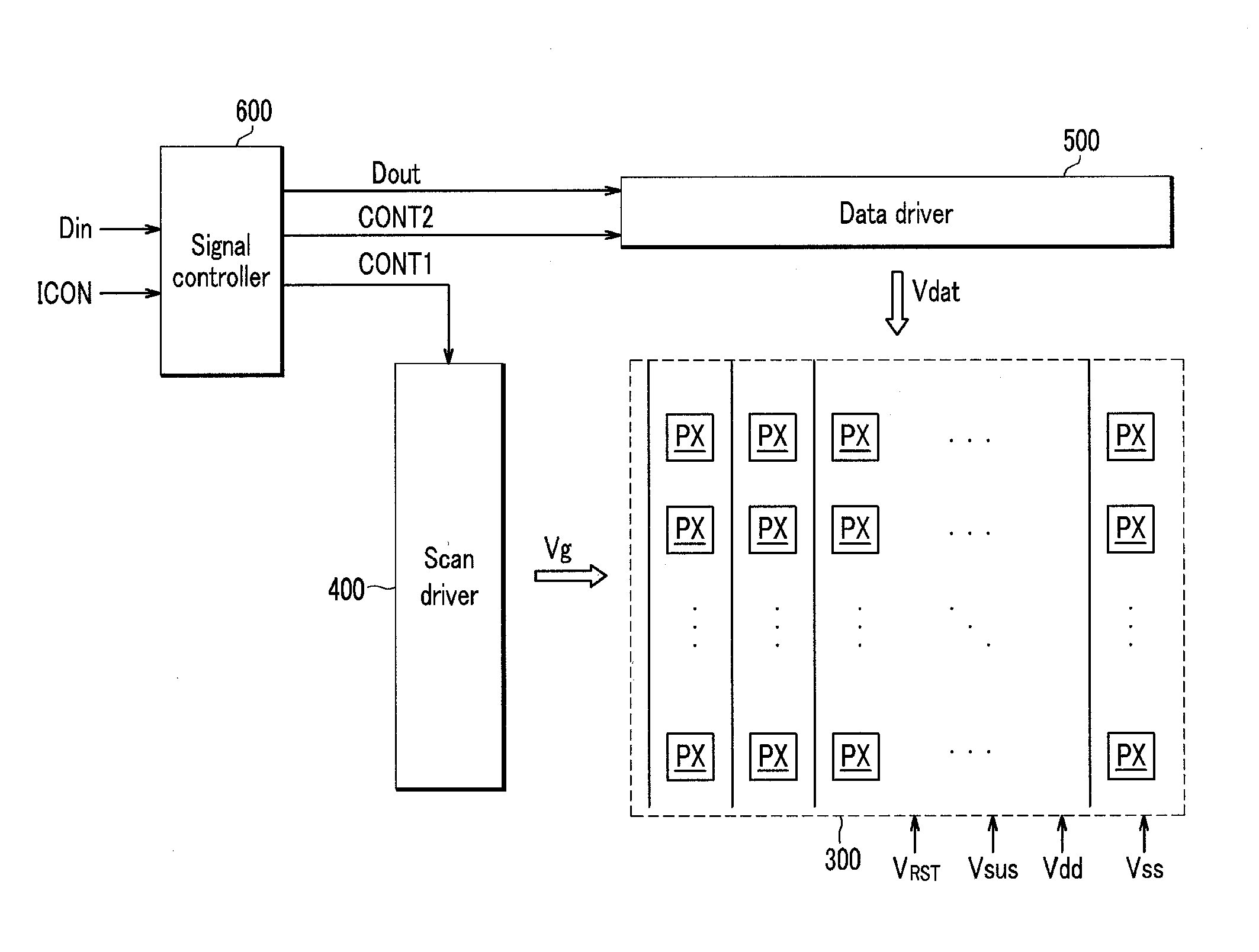
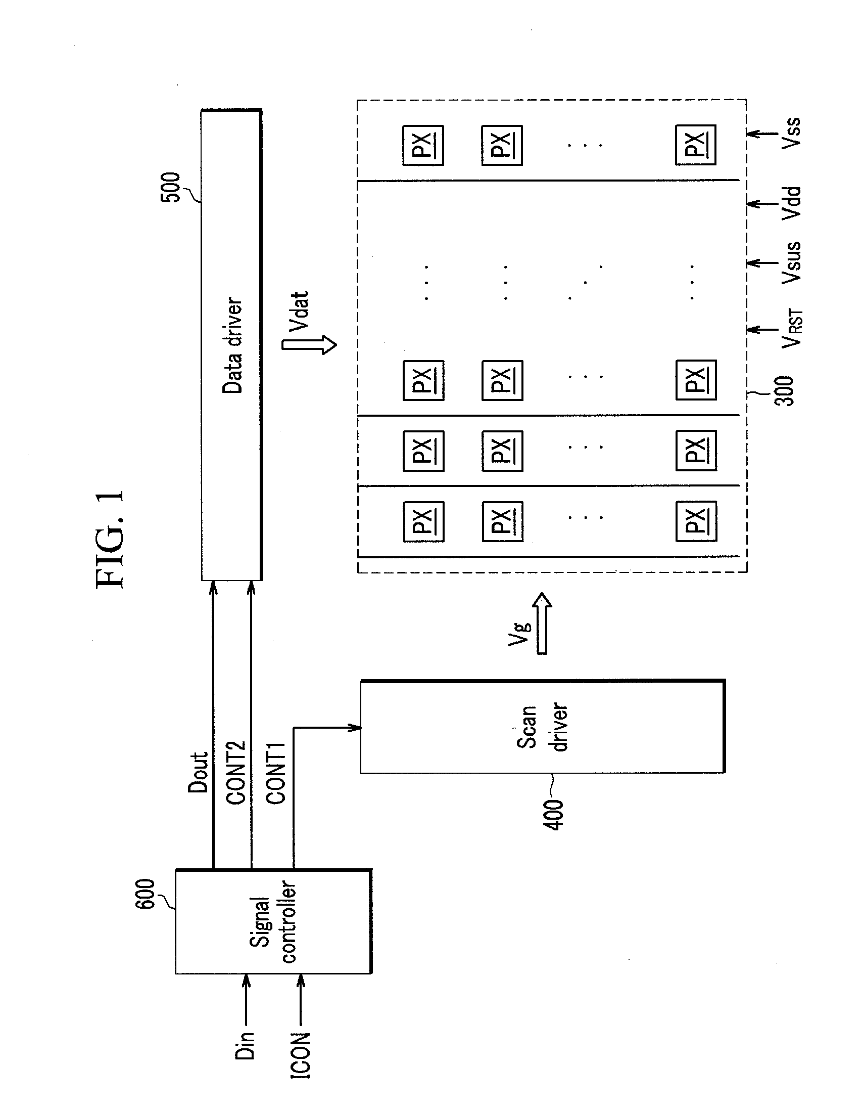
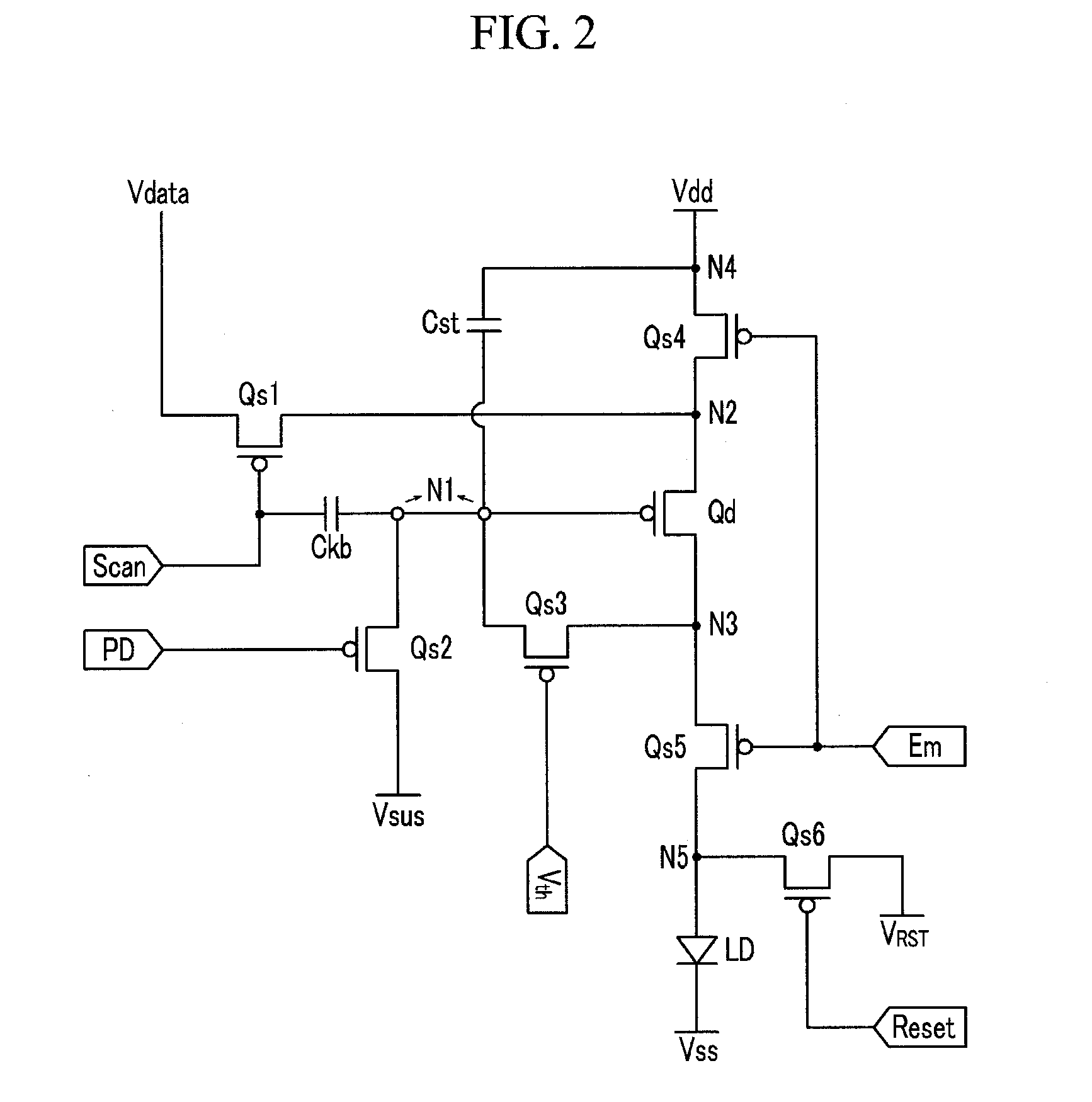
[0076]An organic light emitting device according to an exemplary embodiment of the present invention will now be described with reference to FIG. 1 and FIG. 2. FIG. 1 shows a block diagram of the organic light emitting device, and FIG. 2 shows a circuit diagram of a pixel of the organic light emitting device. The remaining pixels can be identical to the pixel of FIG. 2.

[0077]Referring to FIG. 1, the organic light emitting device includes a display panel 300, a scan driver 400, a data driver 500, and a signal controller 600.

[0078]The display panel 300 includes a plurality of signal lines (not shown), a plurality of voltage lines (not shown), and a plurality of pixels PX connected thereto and arranged substantially in a matrix.

[0079]The signal lines include a plurality of sc...


PUM


Abstract

In a display device, the anode voltage of an organic light emitting element is periodically reset. The control terminal of a driving transistor is periodically reset, and an input data voltage is connected to the control terminal through an input terminal and an output terminal of the driving transistor. As a result, good control over the displayed luminance is achieved. Other features are also provided.

Description

CROSS-REFERENCE TO RELATED APPLICATION[0001]This application claims priority to and the benefit of Korean Patent Application No. 10-2008-0135661 filed in the Korean Intellectual Property Office on Dec. 29, 2008, the entire contents of which are incorporated herein by reference.BACKGROUND OF THE INVENTION[0002](a) Field of the Invention[0003]The present invention relates to a display device and a driving method thereof, and more particularly to an organic light emitting device and a driving method thereof.[0004](b) Description of the Related Art[0005]A hold type flat panel display such as an organic light emitting device displays fixed images for a predetermined time, for example one frame at a time, irrespective of whether or not the images are still images or part of a motion picture. In case of a motion picture, when displaying a moving object, the object is displayed in consecutive frames at discrete consecutive positions in the motion path. Since the frames quickly follow one an...

Claims


Application Information

Patent Timeline
IPC IPC(8): G09G3/30
CPCG09G3/3233G09G2300/0852G09G2300/0861G09G2310/0251G09G2300/0819G09G2310/0256H01L21/02576H01L21/02579
Inventor LEE, BAEK-WOONPARK, SEONG-IIPARK, KYONG-TAE
Owner SAMSUNG DISPLAY CO LTD
Learn More