Probe and probe card for integrated circuit devices using the same

a technology of integrated circuit devices and probe cards, which is applied in the direction of electronic circuit testing, measurement devices, instruments, etc., can solve the problems of collision, short circuit, collision, etc., and achieve the effect of small pitch

Active Publication Date: 2010-07-08
STAR TECH INC
View PDF14 Cites 5 Cited by
  • Summary
  • Abstract
  • Description
  • Claims
  • Application Information

AI Technical Summary

Benefits of technology

[0013]One aspect of the present invention provides a vertical probe and a probe card for integrated circuit devices using the same, the vertical probe having a depressed structure configured to provide vertical displacement to relieve the stress generated as the probe contacts the device under test.
[0016]The conventional cantilever probe cannot be applied to integrated circuit devices with high-density pads since it requires a lateral space to receive the lateral cantilever. In contrast, the vertical probe of the present application does not need the lateral space, can provide variable contact force and can be applied to the integrated circuit devices with high-density pads of very small pitch. In addition, the conventional vertical probe uses the deformation of the probe body itself to provide the vertical displacement for relieving the stress generated as the probe contacts the device under test, but the adjacent probes may contact each other and cause short circuits or collisions if the deformation of the probe body is too large or there is minor misplacement of the probe body. In contrast, the vertical probe of the present application uses the slots to relieve the stress and the slots of the vertical probes can bend to the same side to prevent the vertical probes from contacting each other and causing short circuits or collisions.

Problems solved by technology

The conventional cantilever probe cannot be applied to integrated circuit devices with high-density pads since it requires a lateral space to receive the lateral cantilever.
In addition, the conventional vertical probe uses the deformation of the probe body itself to provide the vertical displacement for relieving the stress generated as the probe contacts the device under test, but the adjacent probes may contact each other and cause short circuits or collisions if the deformation of the probe body is too large or there is minor misplacement of the probe body.

Method used


Image

  • Probe and probe card for integrated circuit devices using the same
  • Probe and probe card for integrated circuit devices using the same
  • Probe and probe card for integrated circuit devices using the same

Examples


Embodiment Construction

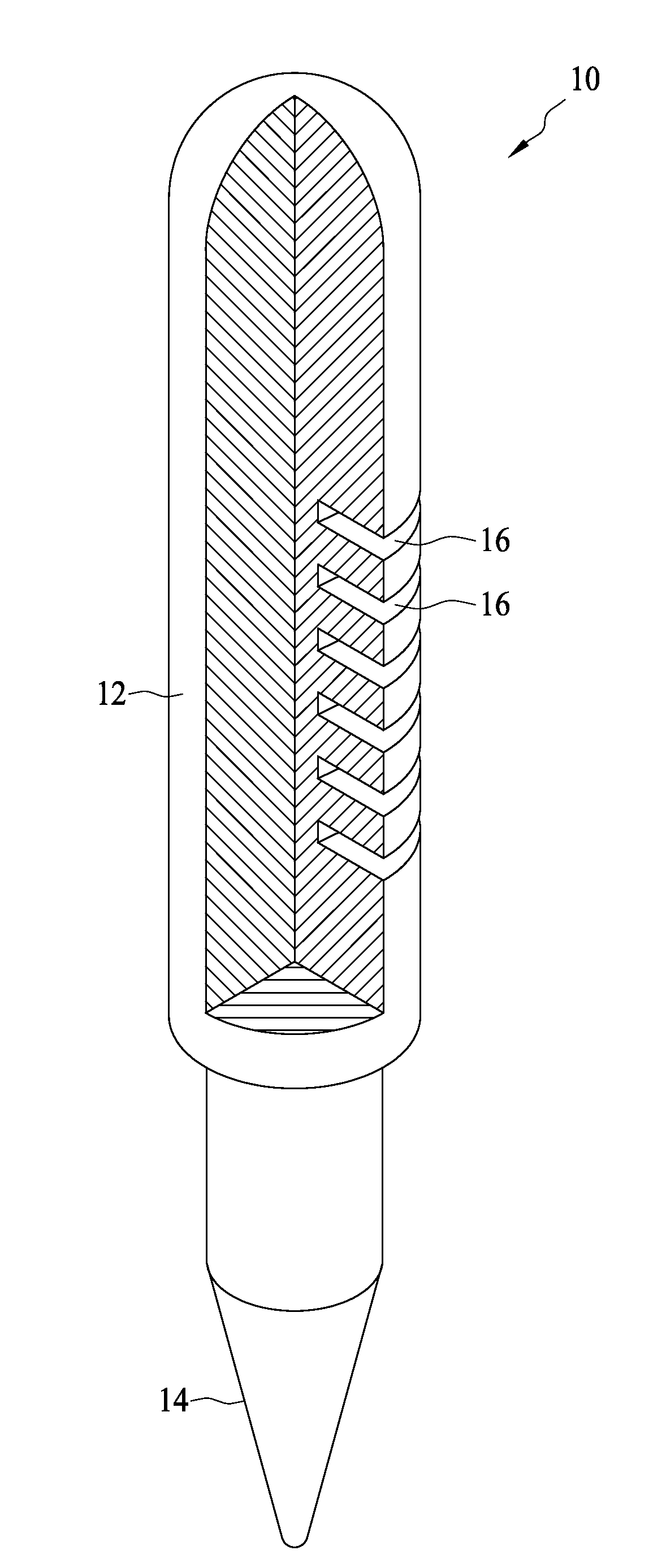
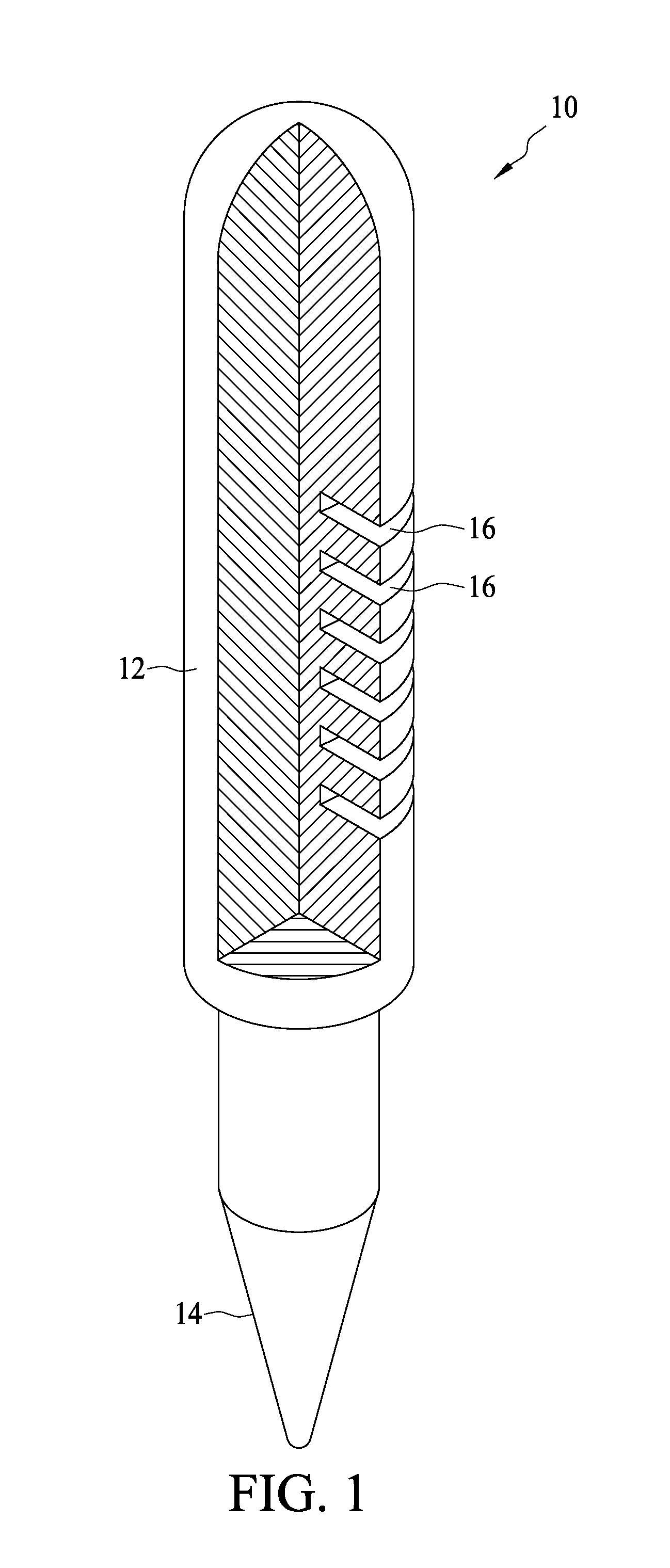
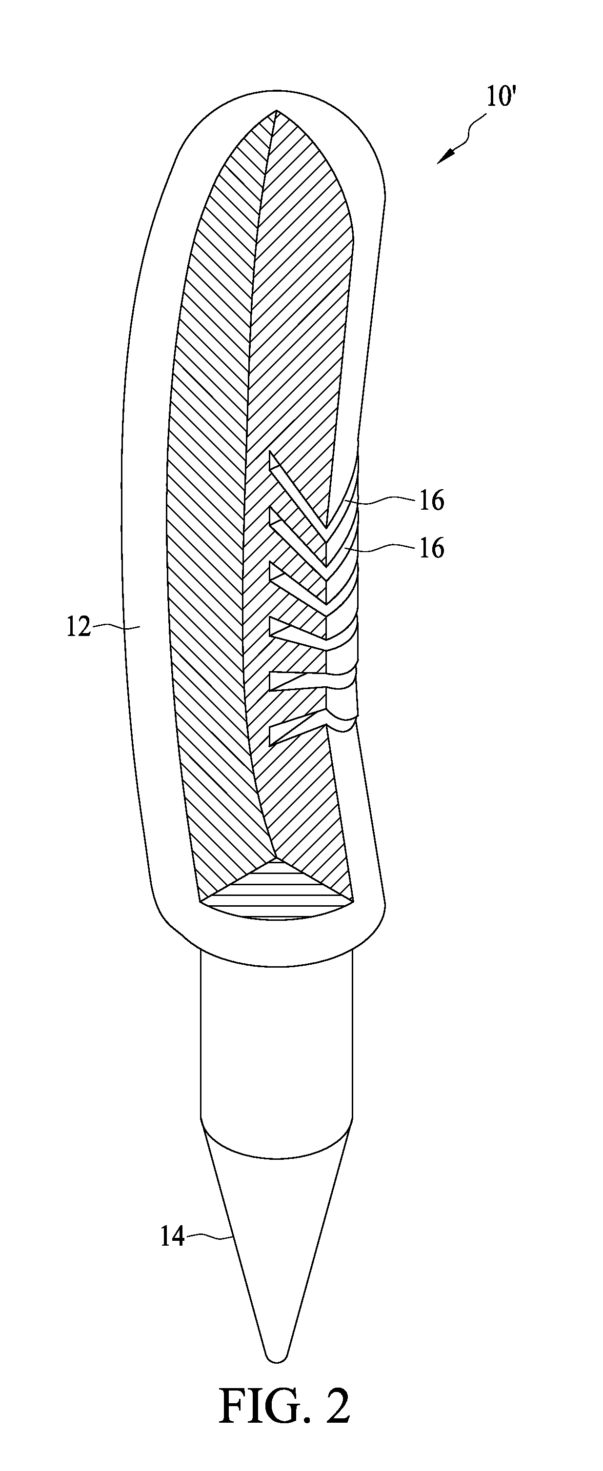
[0023]FIG. 1 illustrates a three-dimensional view of a vertical probe 10 according to one embodiment of the present invention. The vertical probe 10 comprises a linear body 12, a tip portion 14 connected to one side of the linear body 12, and a plurality of slots 16 positioned on the linear body 12. Specifically, the linear body 12 can extend along a direction substantially perpendicular to a device under test. The width of the tip portion 14 can be smaller than the width of the linear body 12. The plurality of slots 16 are configured to facilitate the bending of the linear body 12 when the vertical probe 10 is under compression and is configured to allow the linear body 12 to restore its unbent configuration when the vertical probe 10 is not under compression. Preferably, the linear body 12 is cylindrical, and the slots 16 are fan-shaped. In particular, the fan-shaped slots 16 are perpendicular to the surface of the linear body 12 and positioned on the linear body 12 in parallel su...


PUM


Abstract

A vertical probe comprises a linear body, a tip portion connected to one side of the linear body, and at least one slot positioned on the linear body. In particular, the vertical probe includes a depressed structure having a plurality of slots positioned on the linear body in parallel and on one side of the linear body. The present application also provides a probe card for integrated circuit devices comprising an upper guiding plate having a plurality of fastening holes, a bottom guiding plate having a plurality of guiding holes and a plurality of vertical probes positioned in the guiding holes. The vertical probe includes a linear body positioned in the guiding holes, a tip portion connected to one side of the linear body and at least one slot positioned on the linear body.

Description

CROSS REFERENCE TO RELATED APPLICATIONS[0001]This application is a continuing application of application Ser. No. 12 / 237,698, filed Sep. 25, 2008, which is incorporated herein in their entirety by reference.BACKGROUND OF THE INVENTION[0002](A) Field of the Invention[0003]The present invention relates to a vertical probe and a probe card for integrated circuit devices using the same, and more particularly, to a vertical probe having a depressed structure providing vertical displacement for relieving the stress generated as the vertical probe contacts the device under test and a probe card for integrated circuit devices using the same.[0004](B) Description of the Related Art[0005]Generally, it is necessary to test the electrical characteristics of integrated circuit devices on the wafer level to check whether the integrated circuit device satisfies the product specification. Integrated circuit devices with electrical characteristic satisfying the specification will be selected for the...

Claims


Application Information

Patent Timeline
Patent Type & Authority Applications(United States)
IPC IPC(8): G01R1/067G01R31/02
CPCG01R1/06733G01R1/0675G01R1/07314G01R1/07357
Inventor LOU, CHOON LEONG
Owner STAR TECH INC
Why Eureka
Try Eureka