Wafer level lens replication on micro-electrical-mechanical systems

a micro-electrical-mechanical system and lens technology, applied in the field of forming wafer-level lenses, can solve the problems of complex and expensive possible techniques for joining lenses to associated mems structures

Inactive Publication Date: 2010-07-15
APTINA IMAGING CORP
View PDF10 Cites 195 Cited by
  • Summary
  • Abstract
  • Description
  • Claims
  • Application Information

AI Technical Summary

Problems solved by technology

Possible techniques for joining a lens to an associated MEMS structure can be complex and expensive.

Method used


Image

  • Wafer level lens replication on micro-electrical-mechanical systems
  • Wafer level lens replication on micro-electrical-mechanical systems
  • Wafer level lens replication on micro-electrical-mechanical systems

Examples


Embodiment Construction

[0026]In the following detailed description, reference is made to various embodiments that are described with sufficient detail to enable those skilled in the art to practice them. It is to be understood that other embodiments may be employed, and that various structural or logical changes may be made.

[0027]Embodiments described herein relate to a method of making wafer level integrated lens / MEMS structures by forming wafer-level lenses on wafer level MEMS structures. The integrated wafer level structure can then be further integrated with an imager wafer to form a plurality of imaging devices, which are diced from the wafer to form individual imaging devices having integrated lenses and MEMS structures. The embodiments described herein provide a high-throughput wafer level process that will result in smaller, more reliable, and easier to produce autofocus and zoom systems.

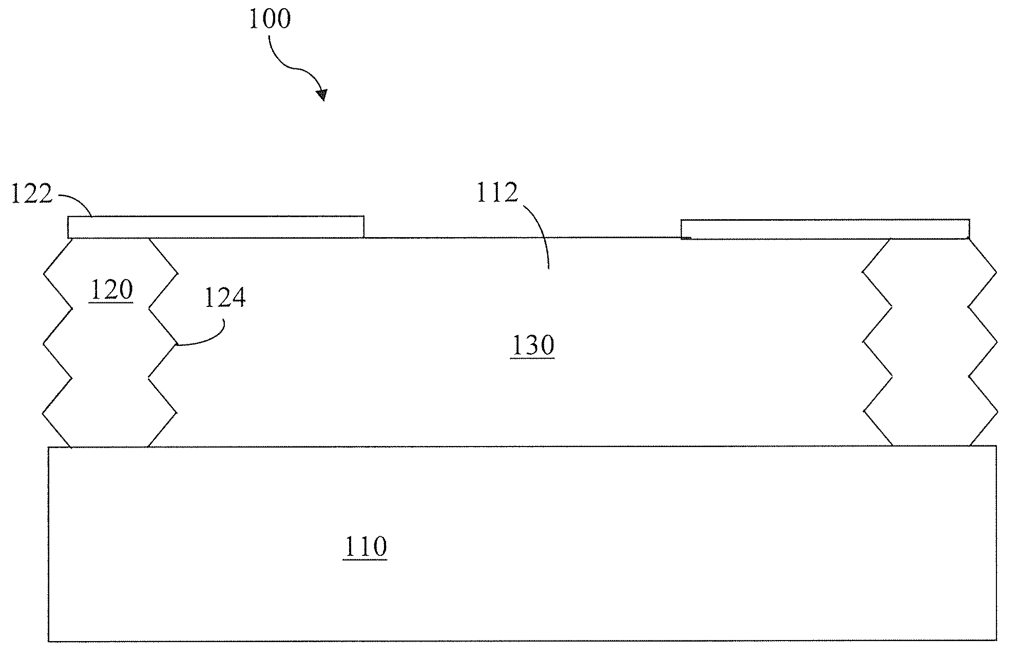
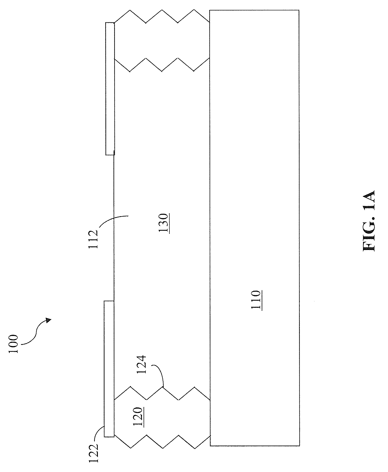
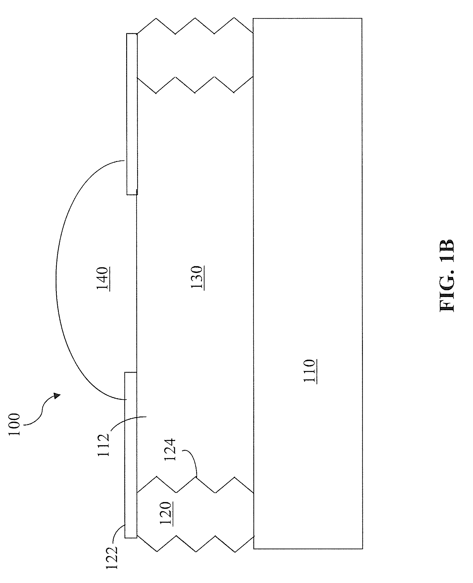
[0028]Now referring to the figures, where like reference numbers designate like elements, FIGS. 1A-1D show an e...


PUM


Abstract

Movable lens structures in which a lens is formed on a micro-electrical-mechanical system and methods of making the same. A method of forming the lens includes forming a micro-electrical-mechanical system on a substrate, arranging a first mold inside the micro-electrical-mechanical system, and forming a lens on the micro-electrical-mechanical system using the first mold.

Description

FIELD OF THE INVENTION[0001]Embodiments described herein relate generally to processes of forming lens wafers for use in imaging devices, and more specifically to processes of forming wafer-level lenses connected to and movable by micro-electrical-mechanical systems (MEMS) technology.BACKGROUND OF THE INVENTION[0002]Microelectronic imaging devices are used in a multitude of electronic devices. As microelectronic imaging devices have decreased in size and improvements have been made with respect to image quality and resolution, they are now commonly found in electronic devices including mobile telephones and personal digital assistants (PDAs) in addition to their uses in digital cameras.[0003]Microelectronic imaging devices include image sensors that typically use charged coupled device (CCD) systems or complementary metal-oxide semiconductor (CMOS) systems, or other semiconductor imaging systems. The lenses for these microelectronic imaging devices may require mobility for operation...

Claims


Application Information

Patent Timeline
Patent Type & Authority Applications(United States)
IPC IPC(8): G02B7/02
CPCG02B3/0075G02B26/0875G02B7/08
Inventor HEGDE, SHASHIKANTDUPARRE, JACQUESLAKE, RICKBOETTIGER, ULRICH C.
Owner APTINA IMAGING CORP
Why Eureka
Try Eureka