Hybrid white organic light emitttng device and method of manufacturing the same

a light emitting diode and hybrid technology, applied in the direction of solid-state devices, electric lighting sources, electric light sources, etc., can solve the problems of light emission loss and achieve the effect of high efficiency

Inactive Publication Date: 2010-07-29
ELECTRONICS & TELECOMM RES INST
View PDF5 Cites 27 Cited by
  • Summary
  • Abstract
  • Description
  • Claims
  • Application Information

AI Technical Summary

Benefits of technology

[0019]According to the present invention, a HOMO level difference between a fluorescent emission layer and an electron transport layer in an organic light emitting diode (OLED) is higher than that between the other layers or a LUMO level difference between a fluorescent emission layer and a hole transport layer is higher than a LUMO level difference between the other layers, so that a recombination region is restricted to a part of an emission layer to obtain high-efficiency fluorescent light emission.
[0020]In addition, according to the present invention, triplet excitons that are not used in a fluorescent emission layer are transferred to an auxiliary emission layer formed to be spaced apart from a recombination region by a predetermined distance to emit light in a different color from the fluorescent emission layer, so that both singlet and triplet excitons generated in the OLED are used to obtain high-efficiency white light emission.

Problems solved by technology

As a result, a loss of light emission may be generated.

Method used


Image

  • Hybrid white organic light emitttng device and method of manufacturing the same
  • Hybrid white organic light emitttng device and method of manufacturing the same
  • Hybrid white organic light emitttng device and method of manufacturing the same

Examples


embodiment 1

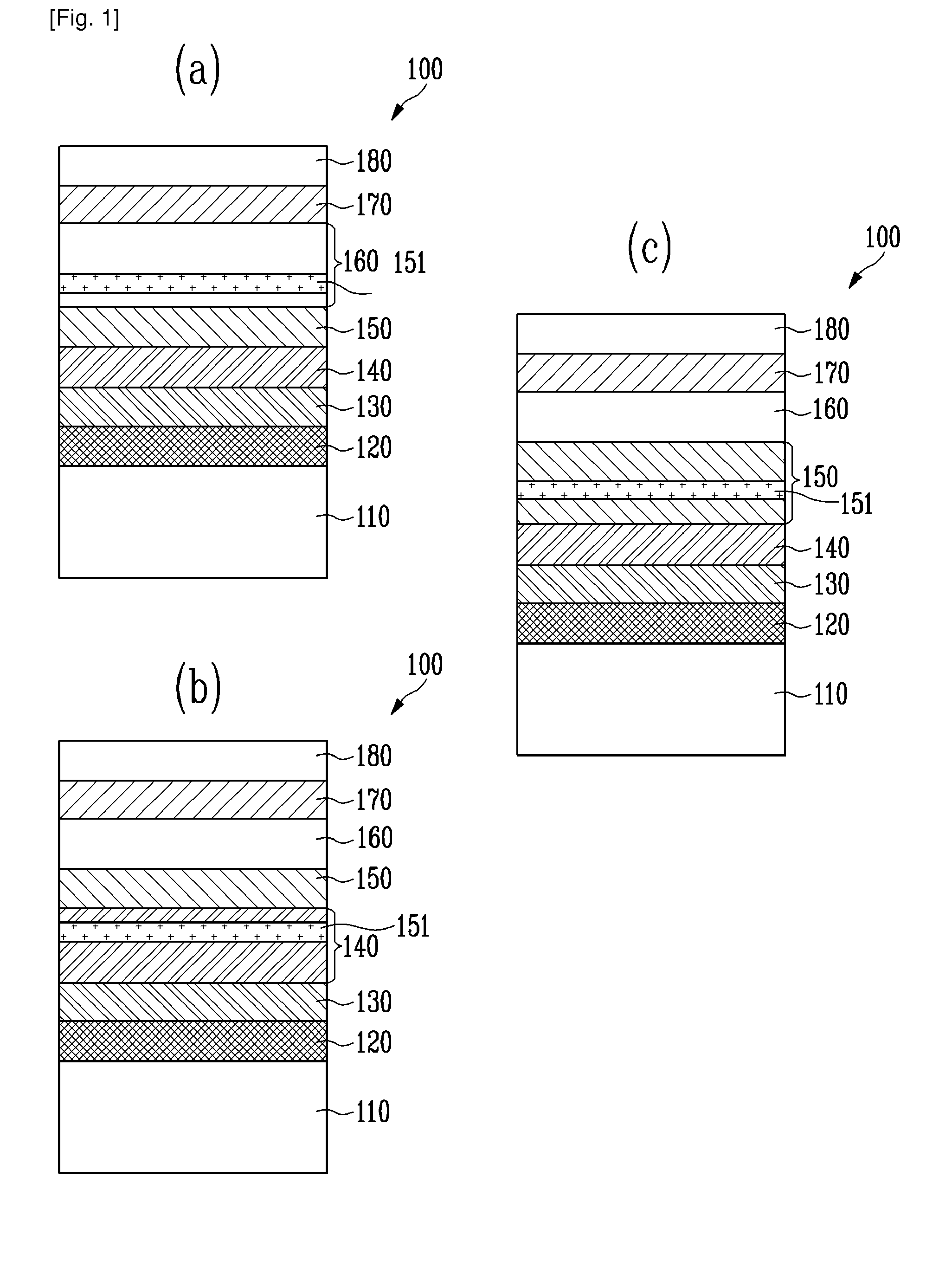
[0026]FIGS. 1A to 1C illustrate a stacked structure of a hybrid white OLED 100 according to a first exemplary embodiment of the present invention.

[0027]As illustrated in FIG. 1A, the hybrid white OLED 100 according to the present invention includes a substrate 110, a first electrode 120, a hole injection layer 130, a hole transport layer 140, a blue / green fluorescent emission layer 150 including a dopant and a host, an electron transport layer 160 formed on the fluorescent emission layer 150 and formed of a material having a higher HOMO level difference with the host of the fluorescent emission layer 150 than that between the other layers, an auxiliary emission layer 151 formed in the electron transport layer 160 and including a dopant and a host, which receive energy from triplet excitons of the fluorescent emission layer 150 and emit light, an electron injection layer 170 and a second electrode 180.

[0028]As described above, the host of the fluorescent emission layer 150 and the el...

embodiment 2

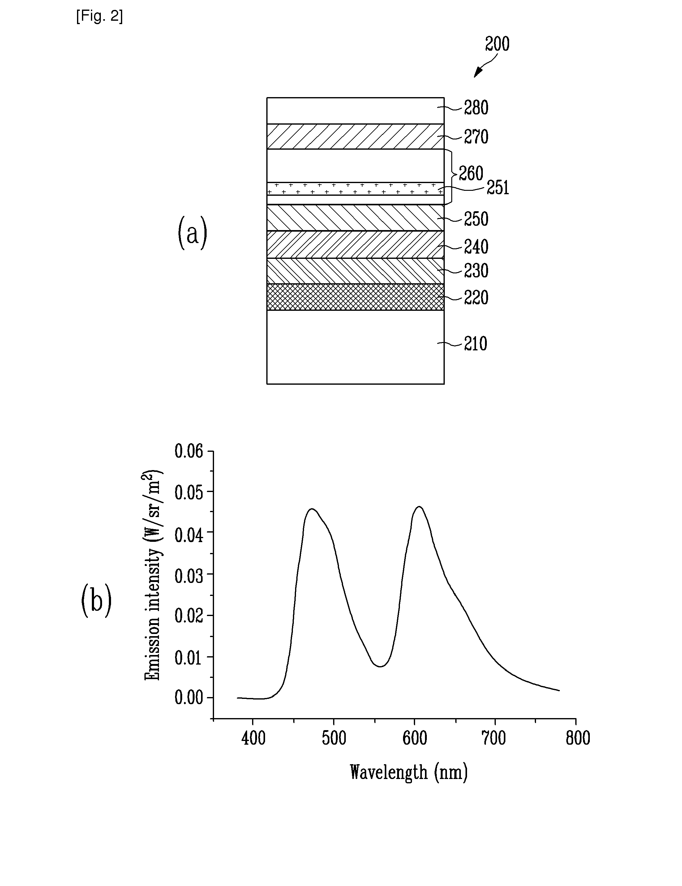
[0039]FIG. 2A illustrates a stacked structure of a hybrid two-wavelength white OLED 200 according to a second exemplary embodiment of the present invention, and FIG. 2B is a graph illustrating light emitting characteristics of the hybrid two-wavelength white OLED illustrated in FIG. 2A.

[0040]Referring to FIG. 2A, the hybrid two-wavelength white OLED 200 according to the present invention includes a substrate 210, a first electrode 220, a hole injection layer 230, a hole transport layer 240, a blue fluorescent emission layer 250, an electron transport layer 260, a red auxiliary emission layer 251, an electron injection layer 270, and a second electrode 280.

[0041]In order to fabricate the hybrid two-wavelength white OLED 200 illustrated in FIG. 2A, first, the substrate 210 is prepared. The substrate 210 may be formed of glass having transparency, quartz, or a flexible panel (e.g., plastic, and a metal thin film), and the first electrode 220 is formed on the substrate 210. The first el...

embodiment 3

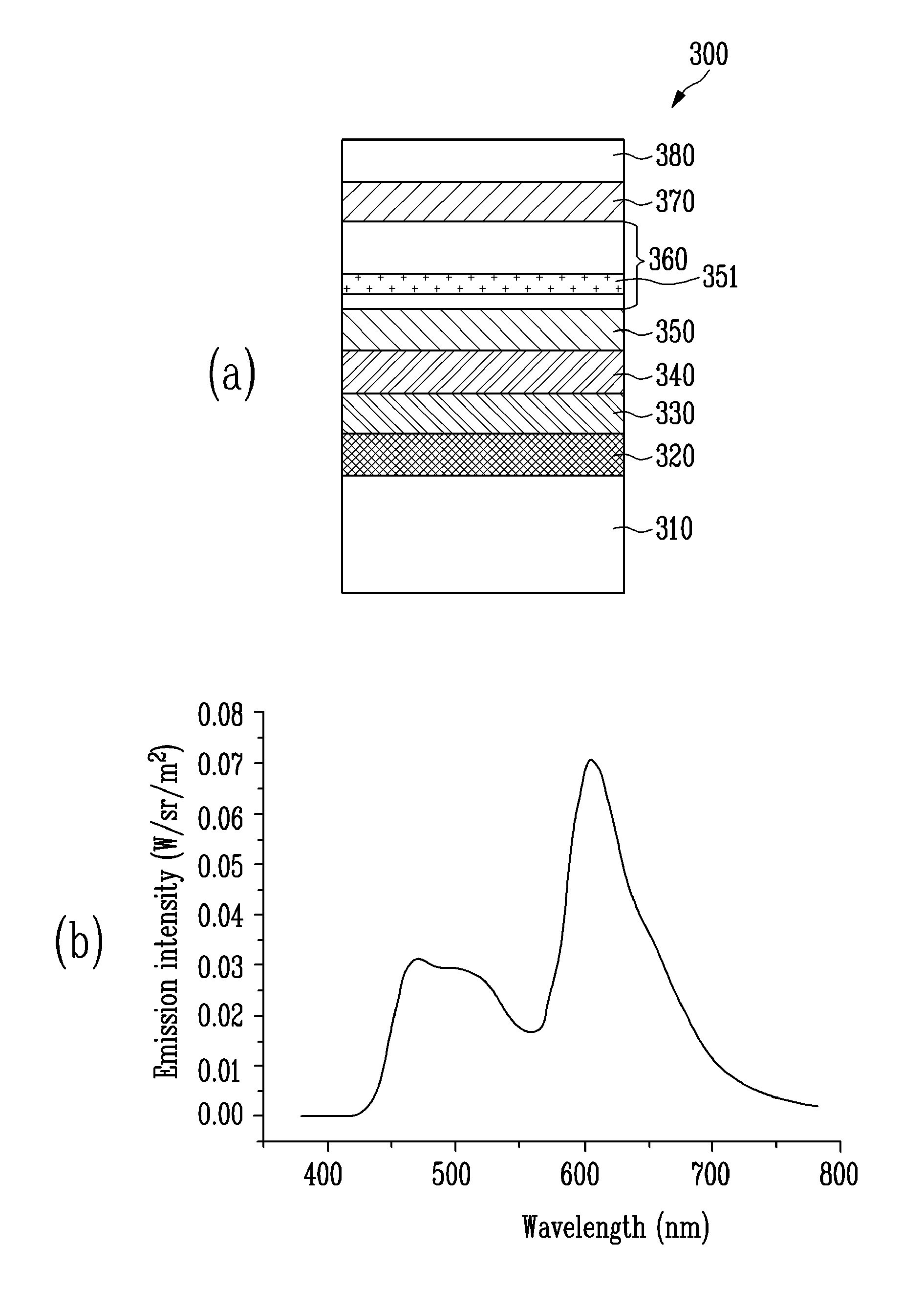
[0051]FIG. 3A illustrates a stacked structure of a hybrid three-wavelength white OLED 300 according to a third exemplary embodiment of the present invention, and FIG. 3B is a graph illustrating light emitting characteristics of the hybrid three-wavelength white OLED 300 illustrated in FIG. 3A.

[0052]Referring to FIG. 3A, the hybrid three-wavelength white OLED 300 according to the present invention includes a substrate 310, a first electrode 320, a hole injection layer 330, a hole transport layer 340, a blue / green fluorescent emission layer 350, an electron transport layer 360, a red auxiliary emission layer 351, an electron injection layer 370, and a second electrode 380.

[0053]In order to fabricate the hybrid three-wavelength white OLED 300 illustrated in FIG. 3A, first, the substrate 310 is prepared. The substrate 310 may be formed of glass having transparency, quartz, or a flexible panel (e.g., plastic, and a metal thin film), and the first electrode 320 is formed on the substrate ...


PUM


Abstract

Provided are a hybrid white organic light emitting diode (OLED) and a method of fabricating the same. A HOMO level difference between a fluorescent emission layer and an electron transport layer in an organic emission layer (OLED) becomes higher than that between the other layers or a LUMO level difference between a fluorescent emission layer and a hole transport layer is higher than that between the other layers, so that a recombination region is restricted to a part of an emission layer to obtain high-efficiency fluorescent light emission. In addition, triplet excitons that are not used in a fluorescent emission layer are transferred to an auxiliary emission layer formed to be spaced apart from a recombination region by a predetermined distance to emit light in a different color from the fluorescent emission layer, so that both singlet and triplet excitons formed in the OLED are used to obtain high-efficiency white light emission.

Description

TECHNICAL FIELD[0001]The present invention relates to a hybrid white organic light emitting diode (OLED) and a method of fabricating the same, and more particularly, to a hybrid OLED and a method of fabricating the same, capable of increasing fluorescent emission efficiency by restricting a charge recombination region to a part of a fluorescent emission layer, and obtaining high-efficiency white light emission using singlet and triplet excitons generated in the fluorescent emission layer.[0002]This work was supported by the IT R&D program of MIC / IITA [2005-S-070-03, Flexible Display].BACKGROUND ART[0003]Recently, the development of a display industry has focused on high resolution as well as compactness in size, light weight and thin thickness using a thin film. To meet such a demand and implement a next generation display, an organic light emitting diode (OLED) technique among existing device manufacturing techniques has been drawing increasing attention, and research into the tech...

Claims


Application Information

Patent Timeline
Patent Type & Authority Applications(United States)
IPC IPC(8): H01L51/52H01L51/56
CPCH05B33/10H05B33/14H05B33/18
Inventor LEE, JEONG IKCHU, HYE YONGCHUNG, SUNG MOOKDO, LEE MIPARK, SANG HEEHWANG, CHI SUN
Owner ELECTRONICS & TELECOMM RES INST
Why Eureka
Try Eureka