Complex memory device and I/O processing method using the same

a memory device and complex technology, applied in the field of memory, can solve the problems of power consumption substantially large, write speed comparablely slow, and subject to the limitation of erase-before-wri

a memory device and complex technology, applied in the field of memory, can solve the problems of power consumption substantially large, write speed comparablely slow, and subject to the limitation of erase-before-wri

US20100191898A1Inactive Publication Date: 2010-07-29SAMSUNG ELECTRONICS CO LTD

Image

  • Complex memory device and I/O processing method using the same
  • Complex memory device and I/O processing method using the same
  • Complex memory device and I/O processing method using the same

Examples


Embodiment Construction

[0031]The following detailed description is provided to assist the reader in gaining a comprehensive understanding of the methods, apparatuses and / or systems described herein. Various changes, modifications, and equivalents of the systems, apparatuses and / or methods described herein will suggest themselves those of ordinary skill in the art. Descriptions of well-known functions and structures are omitted to enhance clarity and conciseness.

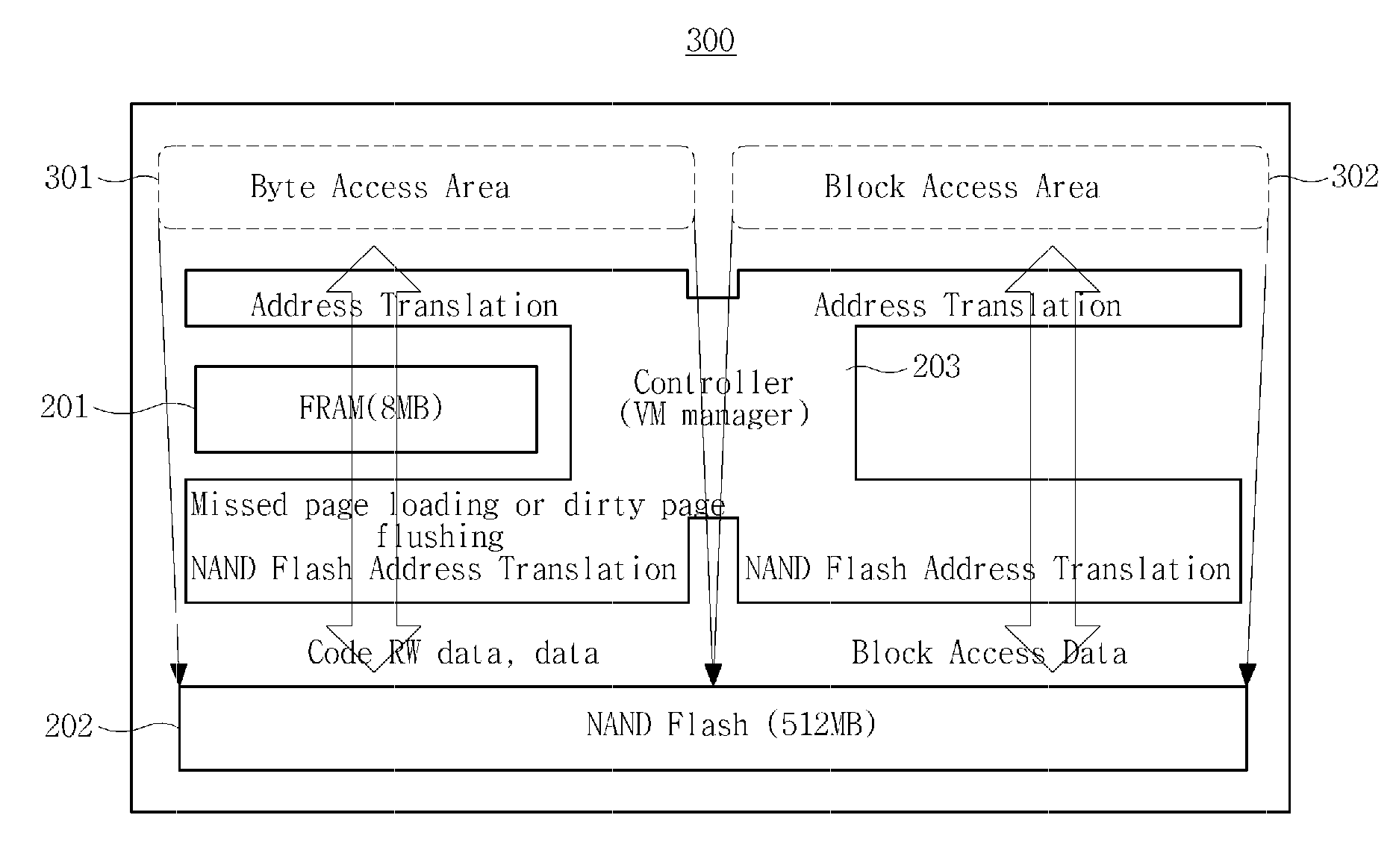
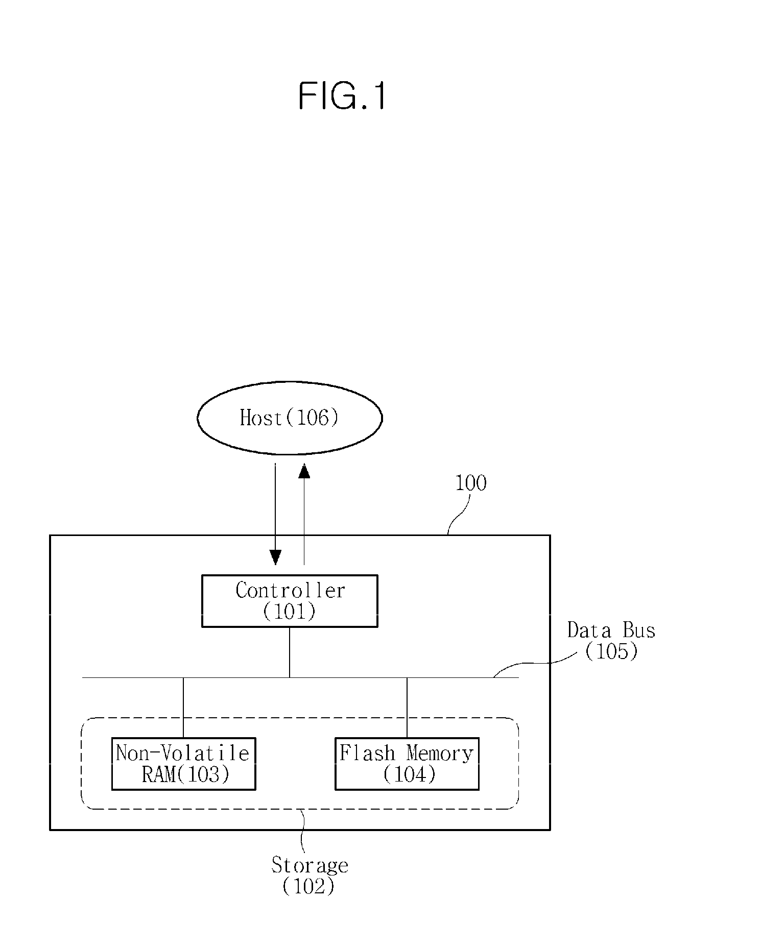
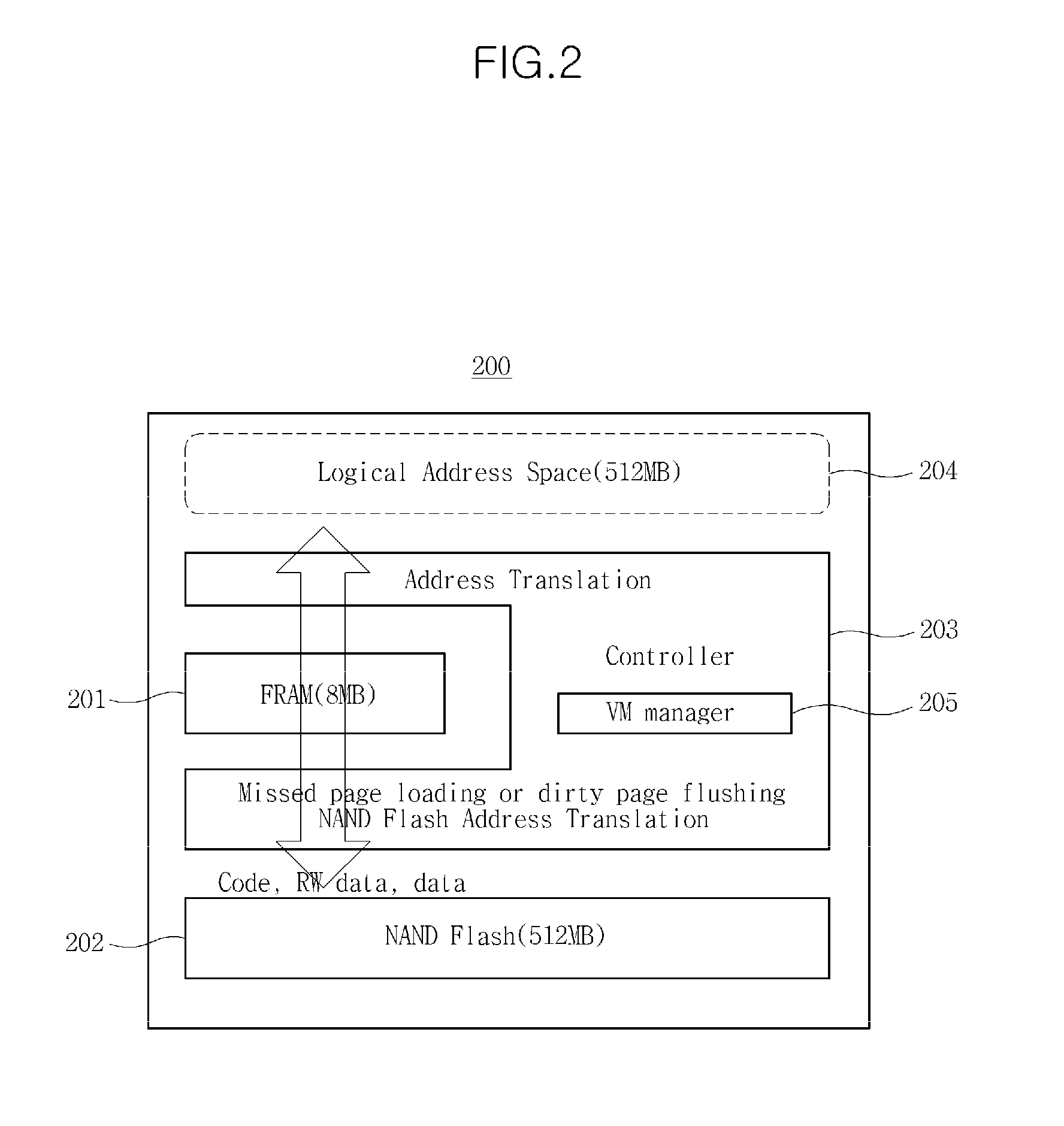
[0032]FIG. 1 is a block diagram illustrating an exemplary complex memory device 100. Referring to FIG. 1, the complex memory device 100 may store various types of data, and may process an input / output request from a host 106. The complex memory device 100 may be configured as a single chip to be communicatably connected to a host 106. In addition, the complex memory device 100 may be implemented inside a computing device which stores and processes data, or may be provided separately to be connectable to and / or detachable from the computing device. ...


PUM


Abstract

A non-volatile mass storage memory and an input / output processing method using the memory are provided. The memory device includes a storage unit including a non-volatile random access memory and a flash memory and a controller to control the storage to process an input / output request. Accordingly, system memories having different purposes and functionalities, such as a flash memory and a dynamic random access memory (DRAM), may be integrated with each other.

Description

CROSS REFERENCE TO RELATED APPLICATION(S)[0001]This application claims the benefit under 35 U.S.C. §119(a) of a Korean Patent Application No. 10-2009-0006178, filed on Jan. 23, 2009, the disclosure of which is incorporated herein in its entirety by reference for all purposes.BACKGROUND[0002]1. Field[0003]The following description relates to a memory, and more particularly, to a configuration of a non-volatile mass storage memory and an input / output processing method using the mass storage non-volatile memory.[0004]2. Description of the Related Art[0005]Generally, an embedded system uses a dynamic random access memory (DRAM) as a main memory to run software, a NOR flash memory to store and execute codes, and a NAND flash memory to store user data.[0006]DRAM provides comparably fast read / write speed and enables byte-access, but because DRAM is a volatile memory, power consumption may be substantially large due to a regular refreshing process. Accordingly, DRAM is generally used to sto...

Claims


Application Information

Patent Timeline
29 Jul 2010
Publication
US20100191898A1
IPC
G06F12/02
CPC
G06F12/0246; G06F2212/7203; G06F2212/7201
Inventors
KIM, JIN-KYU; LEE, HYUNG-GYU