Organic light emitting diode display

a light-emitting diode and organic technology, applied in the direction of electroluminescent light sources, thermoelectric devices, electric lighting sources, etc., can solve the problems of display failures and deterioration of organic light-emitting diodes, and achieve the effect of reducing display failures, durability and the life span of the display

Active Publication Date: 2010-08-12
SAMSUNG DISPLAY CO LTD
View PDF12 Cites 63 Cited by
  • Summary
  • Abstract
  • Description
  • Claims
  • Application Information

AI Technical Summary

Benefits of technology

[0011]The present embodiments provide an organic light emitting diode display having advantages of preventing external moisture and oxygen from intruding into the thin film encapsulation layer and deteriorating the organic light emitting diodes.
[0023]With an organic light emitting diode display according to an embodiment, the thin film encapsulation layer contacts the nonorganic layer at the edge thereof, thereby effectively preventing the external moisture and oxygen from intruding into the thin film encapsulation layer along the edge of the thin film encapsulation layer. Accordingly, the organic light emitting diodes are prevented from being deteriorated so that the display failures can be reduced, and the durability and the life span of the display can be enhanced.

Problems solved by technology

However, an organic light emitting diode may be deteriorated due to internal and external factors.
Consequently, during the process of driving the organic light emitting diode display, the organic light emitting diodes placed at the edge of the display area are deteriorated so that display failures may occur.

Method used


Image

  • Organic light emitting diode display
  • Organic light emitting diode display
  • Organic light emitting diode display

Examples


Embodiment Construction

[0033]The present embodiments will be described more fully hereinafter with reference to the accompanying drawings, in which exemplary embodiments are shown. As those skilled in the art would realize, the described embodiments may be modified in various different ways, all without departing from the spirit or scope of the present embodiments.

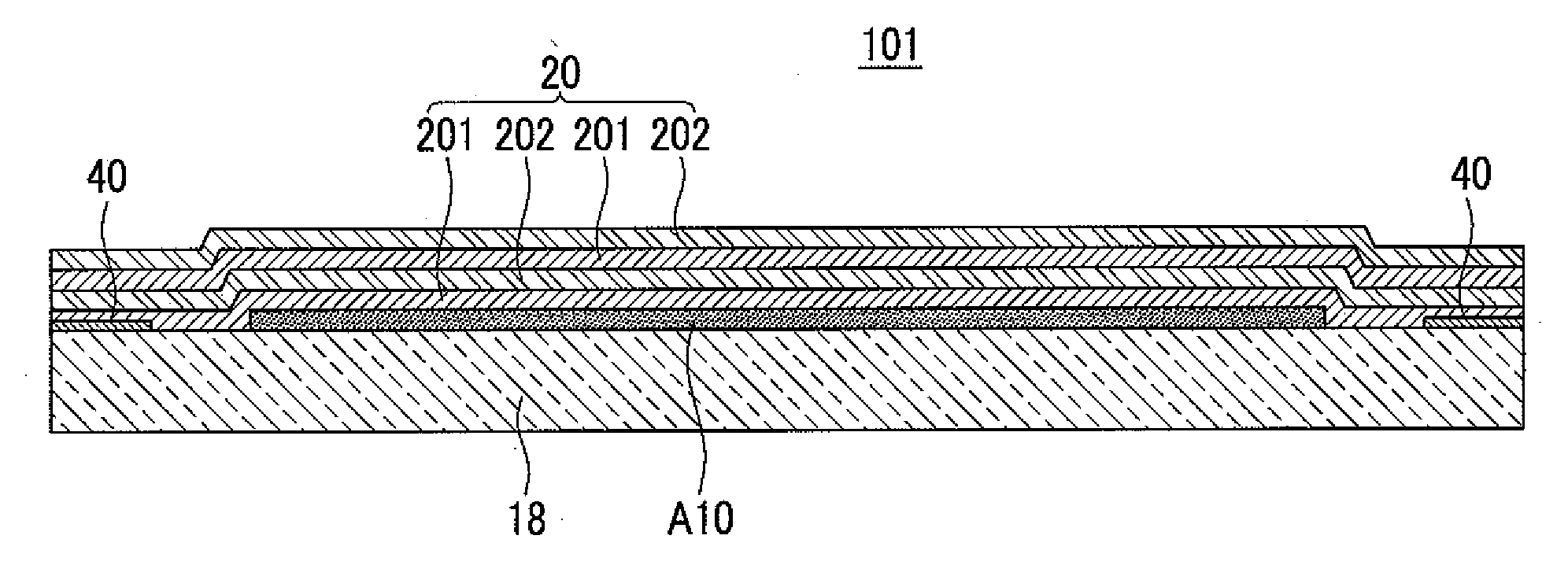
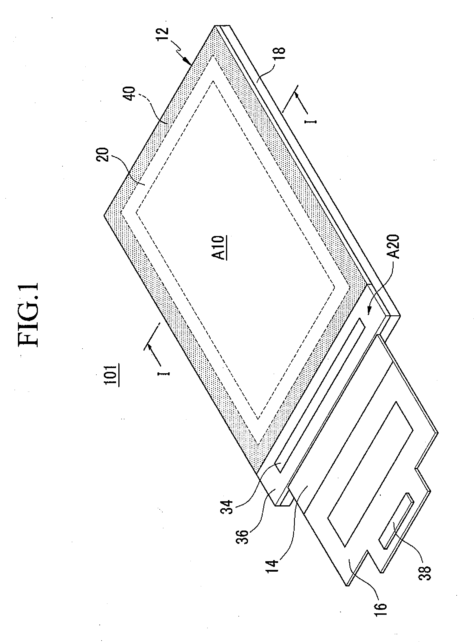
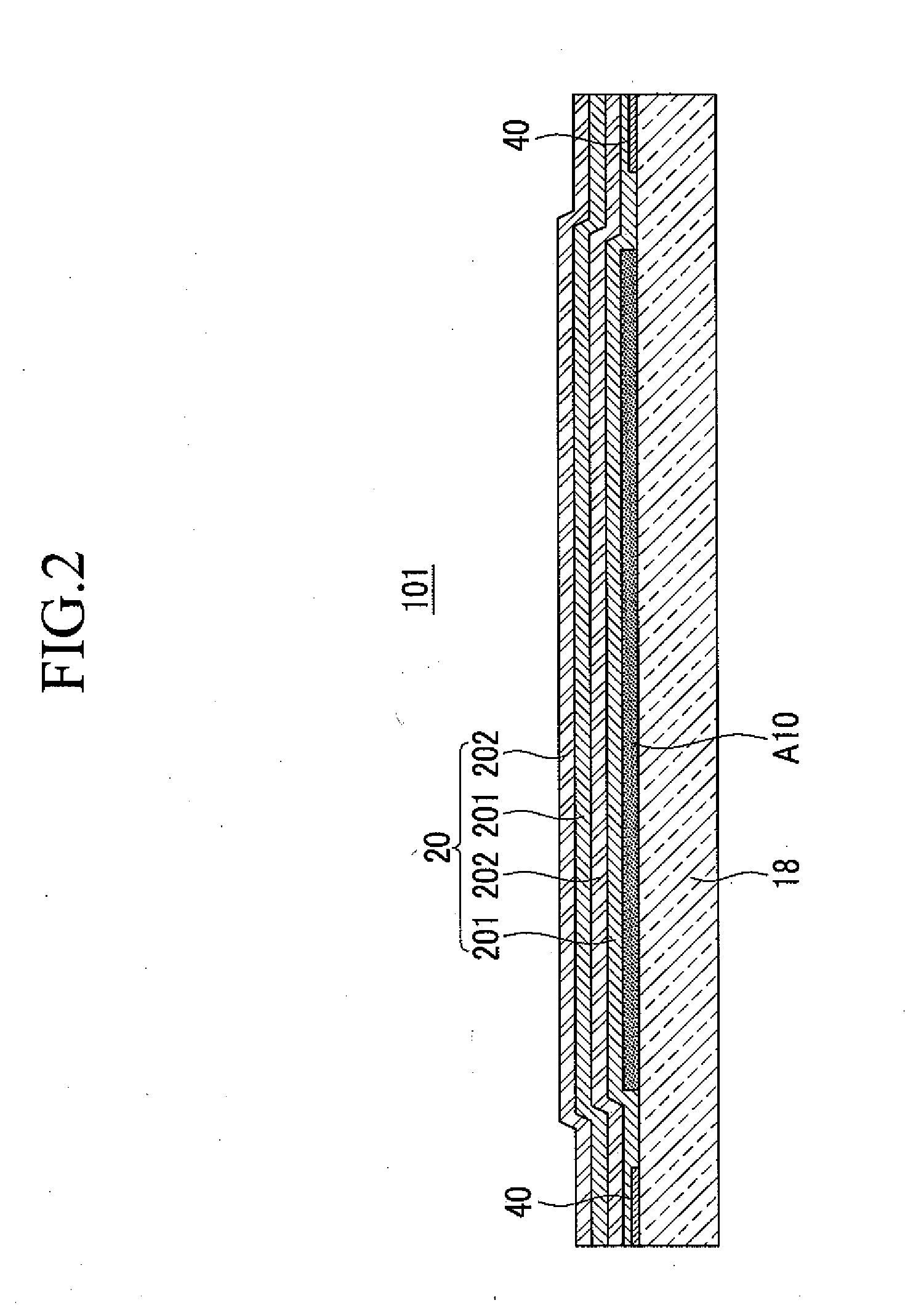
[0034]FIG. 1 is a perspective view of an organic light emitting diode display according to a first exemplary embodiment, and FIG. 2 is a cross-sectional view of the organic light emitting diode display taken along the I-I line of FIG. 1.

[0035]Referring to FIG. 1 and FIG. 2, an organic light emitting diode display 101 according to the present exemplary embodiment includes a panel assembly 12 having a display area A10 and a pad area A20 and displaying a predetermined image at the display area A10, and a printed circuit board 16 electrically connected to the panel assembly 12 via a flexible circuit board 14.

[0036]The panel assembly 12 includes a su...


PUM


Abstract

An organic light emitting diode display includes a substrate having organic light emitting diodes thereon. A thin film encapsulation layer is formed on the substrate such that the thin film encapsulation layer covers the organic light emitting diodes. A nonorganic layer is formed under the thin film encapsulation layer along the edge of the thin film encapsulation layer.

Description

CROSS-REFERENCE TO RELATED APPLICATION[0001]This application claims priority to and the benefit of Korean Patent Application No. 10-2009-0010100 filed in the Korean Intellectual Property Office on Feb. 9, 2009, the entire contents of which are incorporated herein by reference.BACKGROUND OF THE INVENTION[0002]1. Field of the Invention[0003]The present embodiments relate to an organic light emitting diode display, and more particularly, to an organic light emitting diode display having a thin film encapsulation (TFE) structure.[0004]2. Description of the Related Art[0005]An organic light emitting diode (OLED) display has a plurality of organic light emitting diodes each with a hole injection electrode, an organic emissive layer, and an electron injection electrode. With the organic light emitting diode display, electrons and holes are combined with each other in the organic emissive layer to thereby generate excitons. When the excitons shift from the excited state to the ground state,...

Claims


Application Information

Patent Timeline
Patent Type & Authority Applications(United States)
IPC IPC(8): H01L51/52
CPCH01L27/3246H01L51/5253H10K59/122H10K59/873H05B33/04H10K50/844
Inventor KWACK, JIN-HOHAN, DONG-WONLEE, KYU-SUNG
Owner SAMSUNG DISPLAY CO LTD
Why Eureka
Try Eureka