Chip resistor and method for making the same

a chip resistor and chip technology, applied in the manufacture of resistor chips, resistor details, resistive material coating, etc., can solve the problems of changing resistance value, even an open-circuit and paralyzing system, and corrosive gas in the environment cannot directly penetrate the main upper electrod

Active Publication Date: 2010-08-12
YAGEO CORP
View PDF2 Cites 21 Cited by
  • Summary
  • Abstract
  • Description
  • Claims
  • Application Information

AI Technical Summary

Benefits of technology

[0013]The barrier layers have the capabilities of anti-sulfuration and anti-corrosion, which can effectively protect the main upper electrodes from sour gas or other corrosive gases, thus overcoming the disadvantages of the conventional art that the chip resistor is easily affected by the outside environment, resulting in changed resistance value, or even an open-circuit and paralyzed system. In...

Problems solved by technology

The barrier layers have the capabilities of anti-sulfuration and anti-corrosion, which can effectively protect the main upper electrodes from sour gas or other corrosive gases, thus overcoming the disadvantages of the conventional art that the chip resistor is easily affected by ...

Method used


Image

  • Chip resistor and method for making the same
  • Chip resistor and method for making the same
  • Chip resistor and method for making the same

Examples


Embodiment Construction

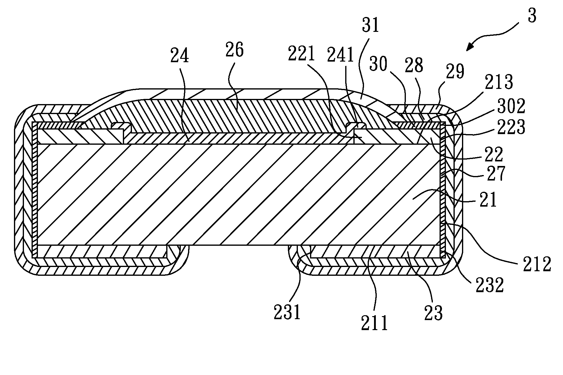
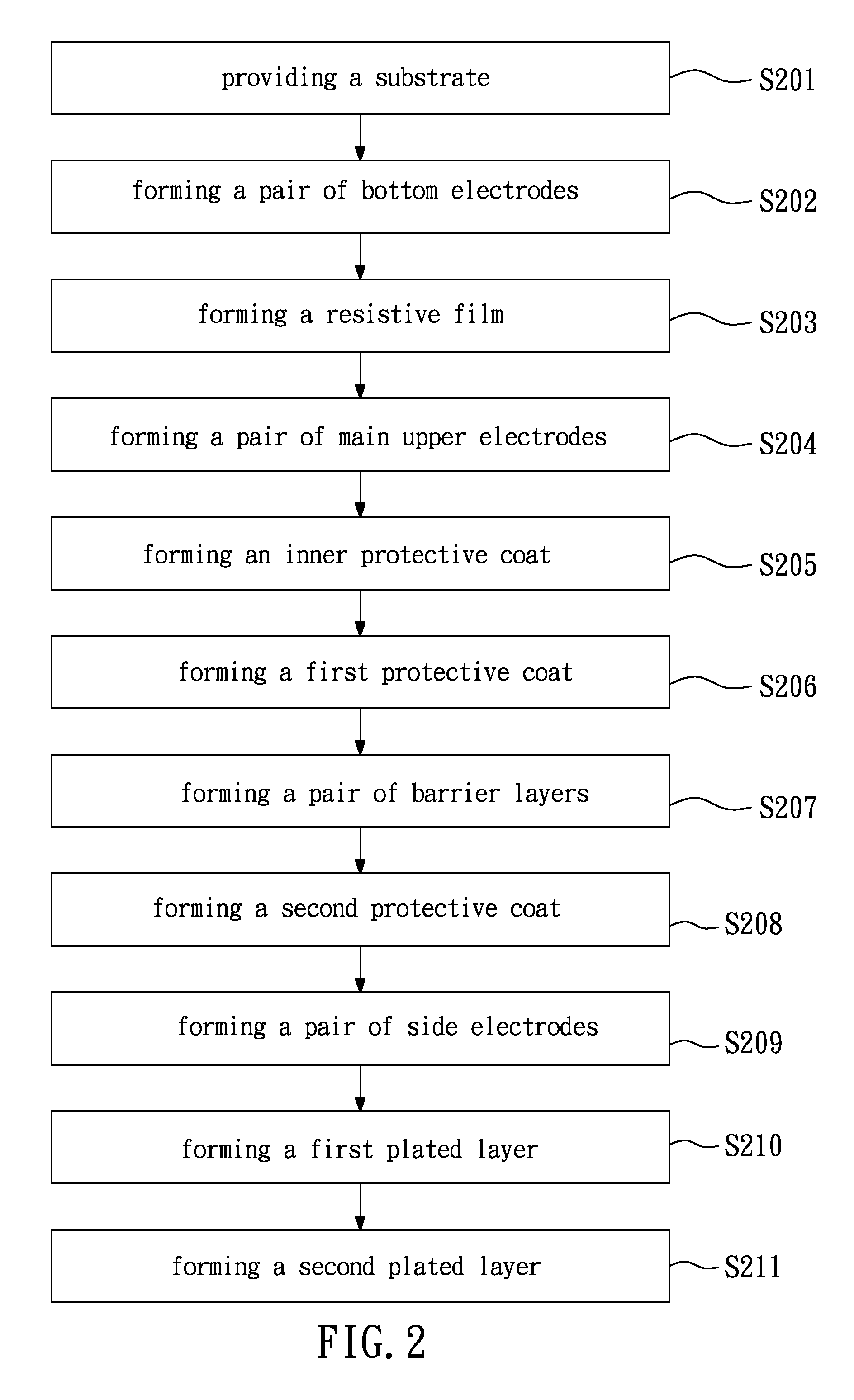
[0018]FIG. 2 shows a schematic flow chart of a method for making a chip resistor according to the first embodiment of the present invention. FIGS. 3a to 3k show schematic cross-sectional views of each step of the method for making the chip resistor according to the first embodiment of the present invention. In this embodiment, a thick film chip resistor is shown.

[0019]Referring to FIGS. 2 and 3a, in Step S201, a substrate 21 is provided, in which the substrate 21 has a back face 211, two side faces 212, and a main face 213.

[0020]Referring to FIGS. 2 and 3b, in Step S202, a pair of bottom electrodes 23 is formed on the back face 211 of the substrate 21. The bottom electrodes 23 are separate from each other and are not connected to each other. Each bottom electrode 23 has an inner side face 231 and an outer side face 232. In the specification of the present invention, “inner side” refers to a direction toward a middle region of the substrate 21, and “outer side” refers to a direction ...


PUM


Abstract

The present invention relates to a chip resistor and method for making the same. The chip resistor includes a substrate, a pair of bottom electrodes, a resistive film, a pair of main upper electrodes, a first protective coat, a pair of barrier layers, a second protective coat, a pair of side electrodes and at least one plated layer. The first protective coat is disposed over the resistive film, and covers part of the main upper electrodes. The barrier layers are disposed on the main upper electrodes, and cover part of the first protective coat. The second protective coat is disposed on the first protective coat, and covers part of the barrier layers. The plated layers cover the barrier layers, the bottom electrodes and the side electrodes. As a result, the chip resistor features high corrosion resistance.

Description

BACKGROUND OF THE INVENTION[0001]1. Field of the Invention[0002]The present invention relates to a chip resistor and a method for making the same, and particularly to a chip resistor having barrier layers and a method for making the same.[0003]2. Description of the Related Art[0004]FIG. 1 shows a schematic cross-sectional view of a conventional chip resistor. The chip resistor 1 is a passive device soldered on an integrated circuit board, and is used for providing resistance. The chip resistor 1 includes a substrate 11, a pair of main upper electrodes 12, a pair of bottom electrodes 13, a resistive film 14, a first protective coat 15, a second protective coat 16, a pair of side electrodes 17, a pair of first plated layers 18, and a pair of second plated layers 19.[0005]The substrate 11 is made of an insulating material, an approximately rectangular plate, and has a back face 111, a pair of side faces 112, and a main face 113. The side faces 112 respectively extend upwards from two o...

Claims


Application Information

Patent Timeline
IPC IPC(8): H01C1/012H01C17/06
CPCH01C1/032H01C1/148Y10T29/49099H01C17/006H01C17/02H01C7/003
Inventor YANG, CHIH-CHUNGWU, WEN-FONLIN, MEI-LINGWU, WEN-CHENGCHEN, TSAI-HUKONG, WEN-HSING
Owner YAGEO CORP
Why Eureka
Try Eureka