Semiconductor storage device and control method of the same

a technology of semiconductor storage and storage device, which is applied in the direction of information storage, static storage, digital storage, etc., can solve the problems of data loss, occurrence of malfunction, and lower throughput speed of pseudo-sram, so as to reliably prevent malfunction and efficiently adjust the sequence of execution

Inactive Publication Date: 2010-08-12
RENESAS ELECTRONICS CORP
View PDF5 Cites 8 Cited by
  • Summary
  • Abstract
  • Description
  • Claims
  • Application Information

AI Technical Summary

Benefits of technology

[0015]The above method is on the basis of the same technical idea as that of the above-described device, and its operational advantage is the same as that of the above-described device.
[0016]As described above, according to the exemplary aspects of an embodiment of the present invention described above, it is possible to efficiently adjust the sequence of executing the refresh operation and the data access operation with respect to each memory bank. It is thereby possible to reliably prevent a malfunction due to interference between the refresh operation and the data access operation without causing degradation of the throughput speed.

Problems solved by technology

However, pseudo-SRAM has a disadvantage of the lower throughput speed than SRAM.
If there is an error in the adjustment, a memory bank on which the data access operation is concentrated is not sufficiently refreshed, for example, which can cause the occurrence of a malfunction such as data loss.
Further, because the data access operation and the refresh operation are performed on different memory banks, if the data access operation is concentrated on a particular memory bank, a case can occur where the memory bank is not refreshed, and it is therefore necessary to impose limits on the data access operation.
In addition, the structure disclosed in Japanese Unexamined Patent Application Publication No. 2002-298574 includes a means of performing a normal access and a refresh one by one in one operation cycle of SRAM, and it does not contribute to improvement on aspects such as accurately adjusting the sequence of executing the both operations and increasing the throughput speed.

Method used


Image

  • Semiconductor storage device and control method of the same
  • Semiconductor storage device and control method of the same
  • Semiconductor storage device and control method of the same

Examples


first exemplary embodiment

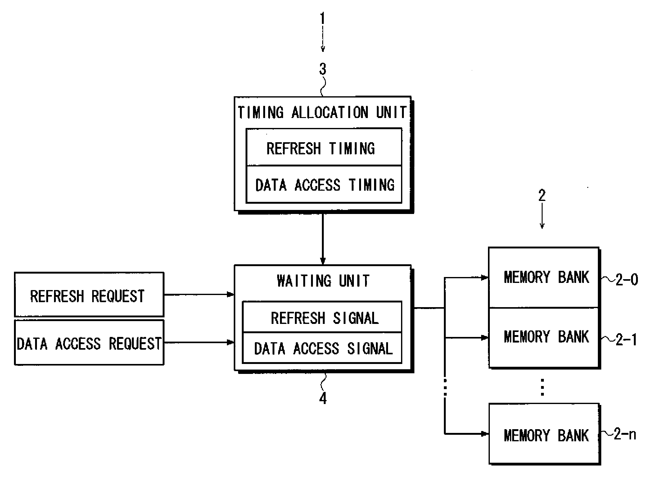
[0032]An exemplary embodiment of the present invention is described hereinafter with reference to the drawings. FIG. 1 shows a functional configuration of a semiconductor storage device 1. The semiconductor storage device 1 is a pseudo-SRAM using DRAM cells, and it includes a memory bank 2, a timing allocation unit 3 and a waiting unit 4.

[0033]The memory bank 2 is an access unit that is composed of a plurality of memory cells. Each of the memory cells has a DRAM configuration that requires a refresh operation to maintain data. A whole memory cell array is made up of a plurality of memory banks 2-0, 2-1 . . . and 2-n. The refresh operation and a data access operation for data writing / reading are performed on each of the memory banks 2-0, 2-1, . . . and 2-n in response to a request signal from a CPU (including an external system), which is not shown.

[0034]The timing allocation unit 3 sets refresh timing to preferentially perform the refresh operation and data access timing to preferen...


PUM


Abstract

A semiconductor storage device includes a timing allocation unit that sets refresh timing to preferentially perform a refresh operation for maintaining data and data access timing to preferentially perform a data access operation for reading or writing the data in accordance with a clock signal with respect to each memory bank including a plurality of memory cells, and a waiting unit that waits start of the data access operation until the data access timing is started in a case where a request for the data access operation is made during the refresh timing and waits start of the refresh operation until the refresh timing is started in a case where a request for the refresh operation is made during the data access timing.

Description

INCORPORATION BY REFERENCE[0001]This application is based upon and claims the benefit of priority from Japanese patent application No. 2009-029365, filed on Feb. 12, 2009, the disclosure of which is incorporated herein in its entirety by reference.BACKGROUND[0002]1. Field of the Invention[0003]The present invention relates to a semiconductor storage device and, particularly, to a technique that prevents interference between a refresh operation and a data access operation in pseudo-SRAM (Static Random Access Memory) using DRAM (Dynamic Random Access Memory) cells.[0004]2. Description of Related Art[0005]Pseudo-SRAM in which a memory cell array is composed of DRAM cells that require a refresh operation for maintaining data and made to function as SRAM is widely used today for its advantages of low cost, high capacity and so on. However, pseudo-SRAM has a disadvantage of the lower throughput speed than SRAM. Further, in order to prevent interference between the refresh operation and a ...

Claims


Application Information

Patent Timeline
Patent Type & Authority Applications(United States)
IPC IPC(8): G11C7/00
CPCG11C11/406G11C11/40618G11C11/40603
Inventor HIROBE, ATSUNORI
Owner RENESAS ELECTRONICS CORP
Why Eureka
Try Eureka