Calibration methods for multiplexed sensor arrays

Inactive Publication Date: 2010-08-12
UNIV OF SOUTHERN CALIFORNIA
View PDF82 Cites 11 Cited by
  • Summary
  • Abstract
  • Description
  • Claims
  • Application Information

AI Technical Summary

Benefits of technology

[0006]Various embodiments include a method of calibrating a nanosensor comprising providing a nanosensor comprising an analyte binder attached to a reference binder, extracting a calibration curve from binding a reference material to the reference binder, and calibrating the nanosensor by using the calibration curve to correct for device variation. In another embodiment, the analyte binder comprises a polynucleotide, polypeptide, aptamer and/or antibody. In

Problems solved by technology

However, there is inevitably some device to device variation in performance due in part to random orientation of nanowires over the surface of the nanosensor.
Variable numbers of such binding groups between different devices in the array will cause a divergence in the properties of the devices within the array.

Method used


Image

  • Calibration methods for multiplexed sensor arrays
  • Calibration methods for multiplexed sensor arrays
  • Calibration methods for multiplexed sensor arrays

Examples


example 1

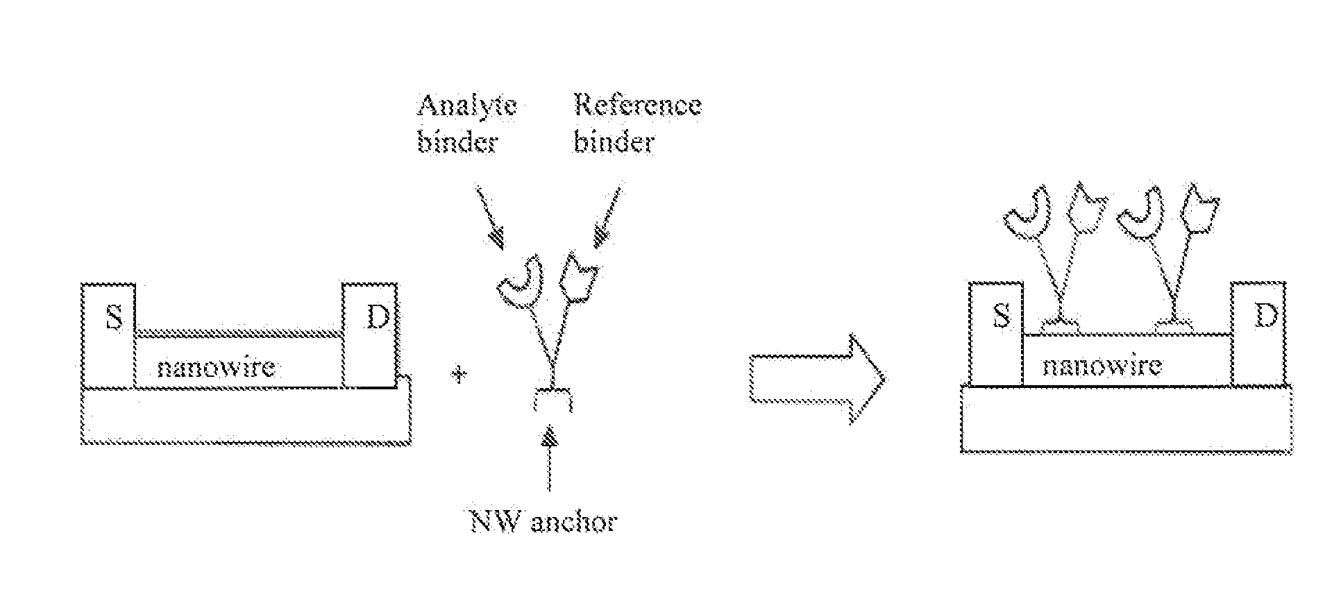
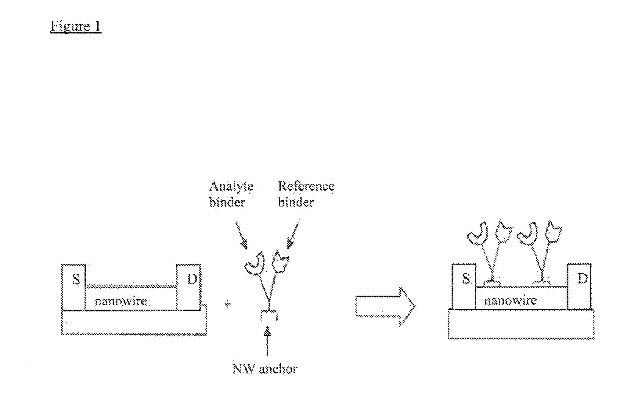
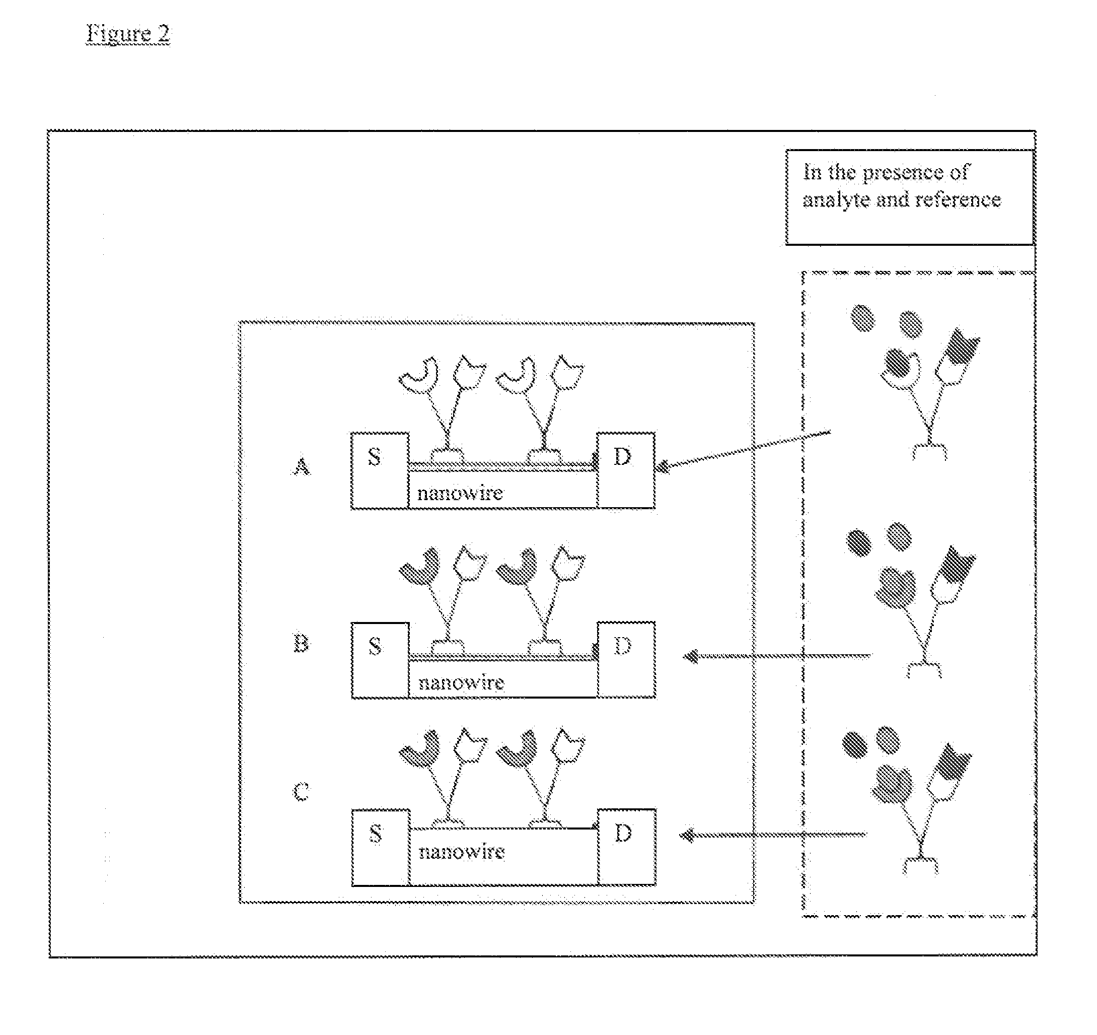
General Makeup of a Sensor Array

[0025]The sensing element in the arrays may be a nanowire based field effect transistor (FET). FETs of this type are very sensitive to their environment. Since the semiconducting material in the channel of the FET is a nanowire (NW), small changes in the environment around the NW, such as temperature, pressure, ionic strength for solutions in contact with the wire, etc., lead to marked changes in the conductance of the NW and thus the performance of the FET. NW based FETs have been prepared with carbon nanotubes and a range of NW materials, such as Si, In2O3 and others. These devices have been used as chemical sensors for both gaseous and solution samples. While these FETs are sensitive to their environment, they are not selective for a specific analyte. In order to generate a biosensor, the surface of the nanowire is coated with a molecule or biomaterial that selectively binds a desired analyte. This binding agent will selectively bind the analyte of...

example 2

Preparing a Multiplexed Array

[0026]To prepare a multiplexed array capable of detecting several biomolecules simultaneously, different devices must be coated with different binding agents. The agents may be, for example, oligonucleotides, antibodies, aptamers, or any other material that will bind the target analyte with high affinity and high specificity. Thus, if an array of ten devices is prepared and each coated with a different binding agent, this array could be used to measure the levels of ten different biomaterials at once. If the ten devices are placed close together on the substrate, this array can be coupled with a microfluidic delivery system and used to analyze very small samples, very rapidly. Thus, multiplexed sensor arrays may be produced that are capable of measuring a large number of biomaterials (potentially 100's or 1000's) in a single sample.

example 3

Preparing an FET Array

[0027]The FET array may be prepared by synthesizing NW materials in bulk, depositing them uniformly on the substrate and add source and drain electrodes on top of the substrate coated with NWs. This method requires that the NWs be uniformly dispersed over the surface, so that each pair of source and drain electrodes have a similar number of NWs in the channel. There will be some variation, since the NWs are randomly oriented over the surface. Adjusting the NW density on the surface and the source-drain structure, it is possible to make arrays where all of the devices have 10's of NWs in the channel. This variation in NW number between devices leads to device arrays that give channel conductance values within a factor of ten of each other. This was demonstrated for an array of 24 devices.


PUM


Abstract

The present invention relates to the calibration of devices using a secondary binding agent or reference material. In one embodiment, the present invention provides a method of calibrating a nanosensor by providing a nanosensor comprising an analyte binder attached to a reference binder, extracting a calibration curve from binding a reference material to the reference binder, and calibrating the nanosensor by using the calibration curve to correct for device variation.

Description

CROSS-REFERENCE TO RELATED APPLICATIONS[0001]The present application claims the benefit of priority under 35 U.S.C. §119(e) of provisional application Ser. No. 61 / 112,287, filed Nov. 7, 2008, the contents of which are hereby incorporated by reference.GOVERNMENT RIGHTS[0002]This invention was made with U.S. Government support on behalf of the National Institutes of Health by NIH-RO1 grant EB-008275. The U.S. Government may have certain rights in this invention.FIELD OF THE INVENTION[0003]This invention relates generally to the fields of nanosensors and multiplexed arrays and, more specifically, to calibration of nanosensor devices.BACKGROUND OF THE INVENTION[0004]All publications herein are incorporated by reference to the same extent as if each individual publication or patent application was specifically and individually indicated to be incorporated by reference. The following description includes information that may be useful in understanding the present invention. It is not an a...

Claims


Application Information

Patent Timeline
IPC IPC(8): C40B40/06C40B40/10G01N35/00
CPCB82Y15/00B82Y35/00G01N35/00693G01N33/54373G01N27/4146
Inventor THOMPSON, MARKROBERTS, RICHARDCOTE, RICHARDZHOU, CHONGWU
Owner UNIV OF SOUTHERN CALIFORNIA
Why Eureka
Try Eureka