Chip package and manufacturing method thereof

a technology of chip and manufacturing method, applied in the field of semiconductor devices, can solve the problems of reducing the effective performance of the device or the whole circuit, affecting reducing the efficiency of the device, so as to achieve the effect of simplifying the manufacturing process

Active Publication Date: 2010-08-19
ADVANCED SEMICON ENG INC
View PDF99 Cites 93 Cited by
  • Summary
  • Abstract
  • Description
  • Claims
  • Application Information

AI Technical Summary

Benefits of technology

[0006]In view of the foregoing, the present invention is directed to a man

Problems solved by technology

For most electronic devices or packages, electromagnetic interference (EMI) is a common but undesirable disturbance that may interrupt, obstruct, degrade or limit the effective performance of the devices o

Method used


Image

  • Chip package and manufacturing method thereof
  • Chip package and manufacturing method thereof
  • Chip package and manufacturing method thereof

Examples


Embodiment Construction

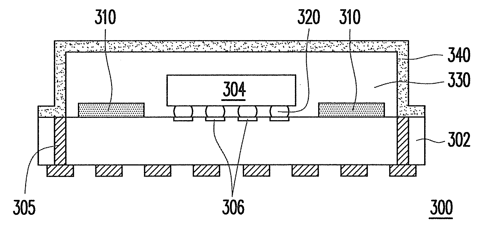
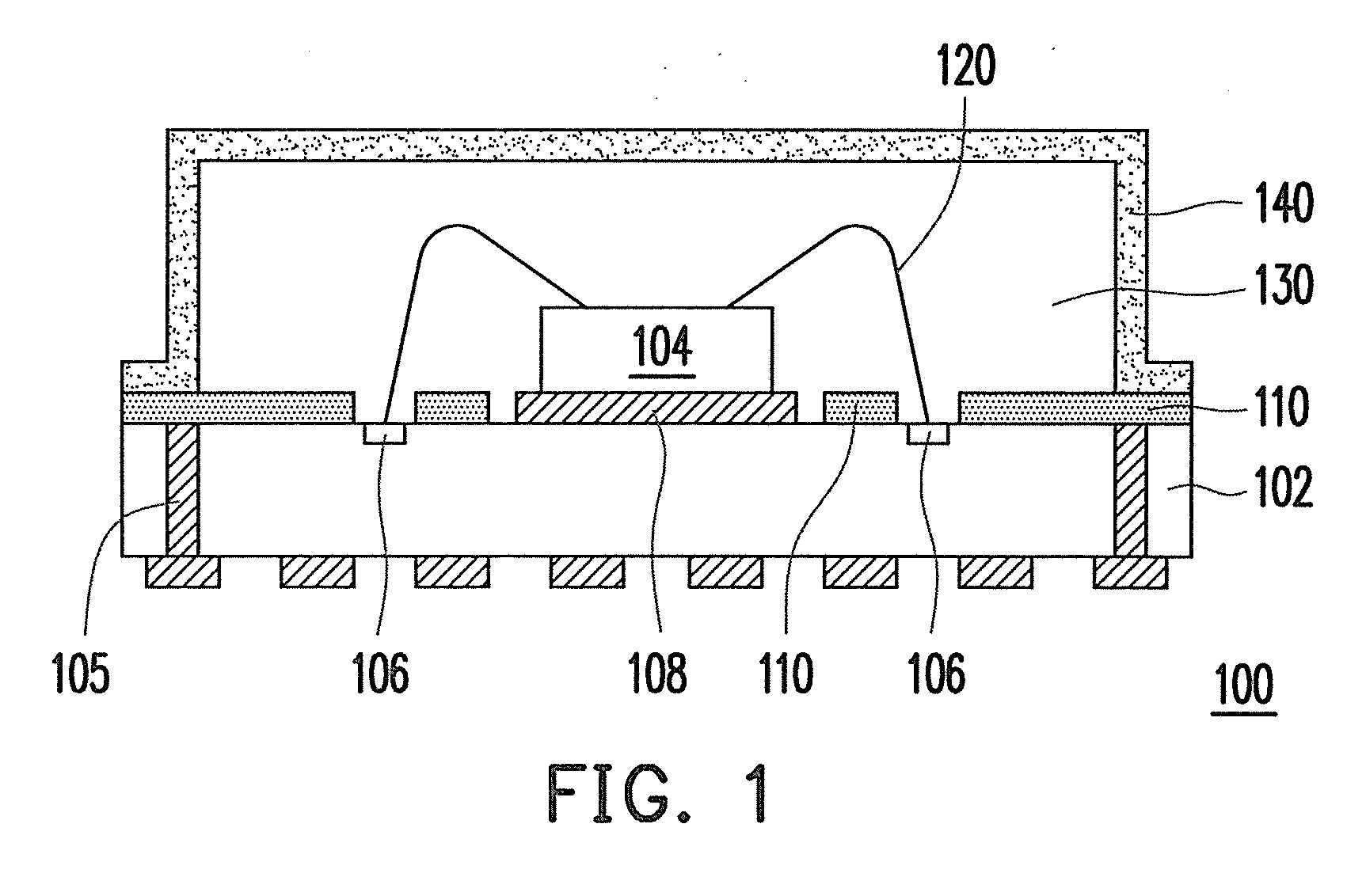
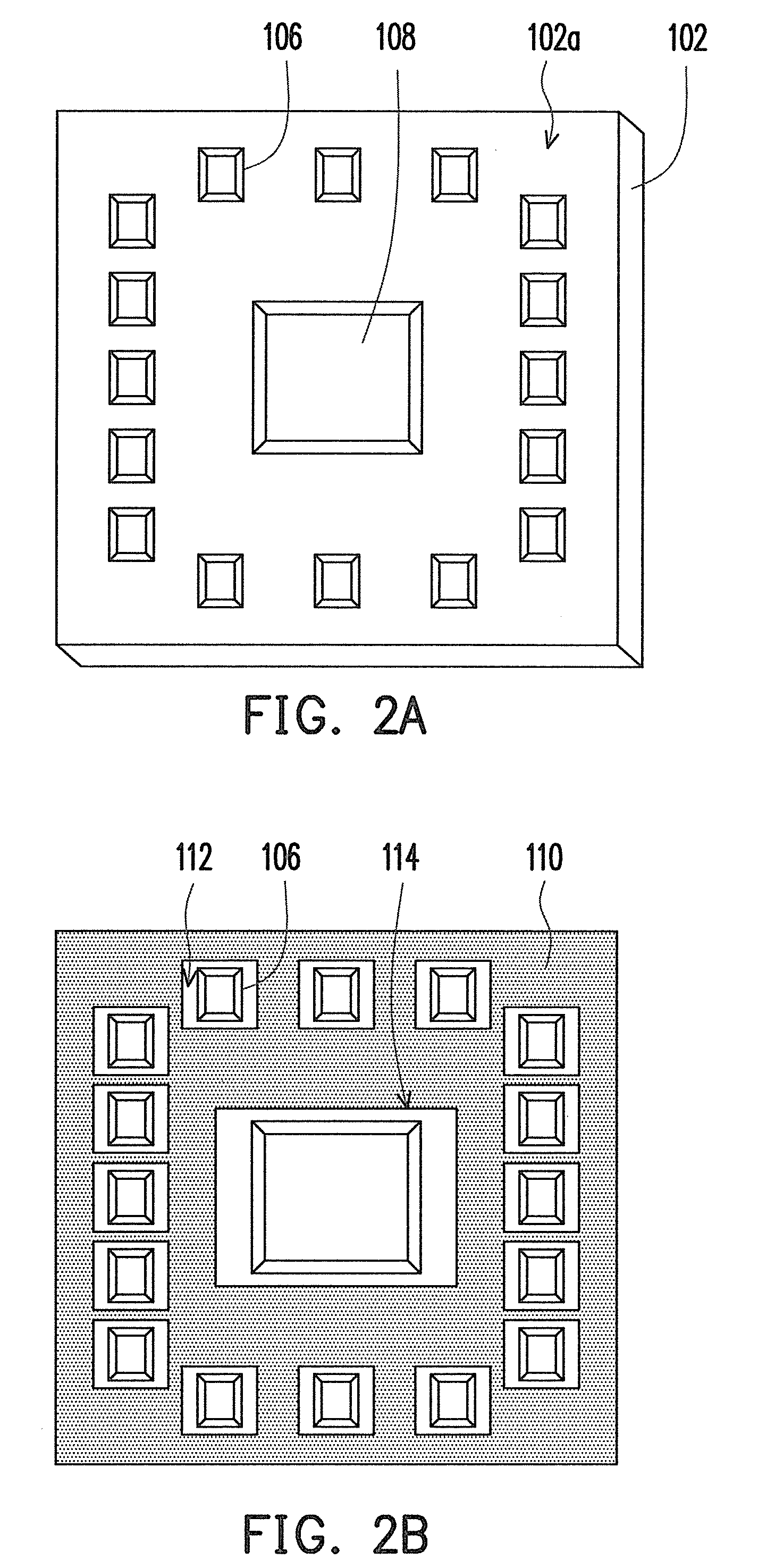
[0018]FIG. 1 is a cross-sectional view of a chip package according to a preferred embodiment of the present invention. Referring to FIG. 1, the chip package 100 of the present embodiment includes a substrate 102, at least a chip 104, a plurality of contacts 106, a first shielding layer 110, a plurality of wires 120, a molding compound 130 and a second shielding layer 140. The substrate 102 can be a laminated substrate, for example, a two-layered laminated PCB substrate. The chip 104 can be a semiconductor chip, for example, a radio-frequency (RF) chip. For example, the material of the contacts 106 may be copper, aluminum, or alloys thereof. For example, the material of the first / second shielding layer may be a solder material, and the material of the first or second shielding layer may be different or the same. The contacts 106 are disposed on the top surface of the substrate 102 and around the die pad 108. The first shielding layer 110 is disposed over the top surface of the substr...


PUM


Abstract

A chip package including at least a shielding layer for better electromagnetic interferences shielding is provided. The shielding layer disposed over the top surface of the laminate substrate can protect the chip package from the underneath EMI radiation. The chip package may further include another shielding layer over the molding compound of the chip package.

Description

BACKGROUND OF THE INVENTION[0001]1. Field of the Invention[0002]The present invention relates to a semiconductor device, and more particularly to a chip package.[0003]2. Description of Related Art[0004]For most electronic devices or packages, electromagnetic interference (EMI) is a common but undesirable disturbance that may interrupt, obstruct, degrade or limit the effective performance of the devices or the whole circuit.[0005]Accordingly, with the increased demand in packaging of high frequency devices, weights for better EMI shielding are raised. Conventionally, extra shielding plate or ground plate may be utilized according to the related art, which results in an excessive thickness of the device and higher manufacturing costs.SUMMARY OF THE INVENTION[0006]In view of the foregoing, the present invention is directed to a manufacturing method of a chip package to simplify the manufacturing process.[0007]The present invention is further directed to a chip package with enhanced eff...

Claims


Application Information

Patent Timeline
IPC IPC(8): H01L23/552H01L21/50
CPCH01L23/055H01L23/3121H01L2924/30107H01L24/48H01L2924/3025H01L23/49827H01L23/552H01L2224/16225H01L2224/48091H01L2224/48227H01L2924/01078H01L2924/19041H01L2924/00014H01L2924/00H01L2924/14H01L2924/00011H01L2224/0401H01L2224/45099H01L2224/45015H01L2924/207
Inventor EUN, YOUNGHYOKIM, DUKMAN
Owner ADVANCED SEMICON ENG INC
Why Eureka
Try Eureka