Chiplet driver pairs for two-dimensional display

a chiplet driver and two-dimensional display technology, applied in semiconductor devices, instruments, computing, etc., can solve the problems of limited number of rows (or columns) of passive-matrix drive devices, power required for non-imaging pre-charge, flicker can become perceptible, etc., to achieve the lowest cost, reduce the number of components and connections, and improve performance

Active Publication Date: 2010-08-19
GLOBAL OLED TECH
View PDF25 Cites 36 Cited by
  • Summary
  • Abstract
  • Description
  • Claims
  • Application Information

AI Technical Summary

Benefits of technology

[0016]The present invention has the advantage that, by providing a display device having a plurality of pixels associated into two-dimensional arrays, each two-dimensional array having distributed, separate row and column chiplet drivers, performance is improved and the number of components and connections is reduced. Further, by having separate row and column driver chiplets, each chiplet can be made with the lowest cost semiconductor fabrication process available for each chiplet.

Problems solved by technology

However, a passive-matrix drive device is limited in the number of rows (or columns) that can be included in the device since the sequential nature of the row (or column) driving creates flicker.
If too many rows are included, the flicker can become perceptible.
Moreover, the currents necessary to drive an entire row (or column) in a display can be problematic the power required for the non-imaging pre-charge and discharge steps of PM driving become dominant as the area of the PM display grows.
These problems limit the physical size of a passive-matrix display.
Thin-film transistors (TFTs) made from amorphous or polycrystalline silicon are relatively large and have lower performance compared to conventional transistors made in crystalline silicon wafers.
Moreover, such thin-film devices typically exhibit local or large-area non-uniformity across the glass substrate that results in non-uniformity in the electrical performance and visual appearance of displays employing such materials.
Since a conventional passive-matrix display design is limited in size and number of light-emitting elements, and an active-matrix design using TFTs has lower electrical performance, there is a need for an improved control method for display devices employing LEDs that overcomes these problems.

Method used


Image

  • Chiplet driver pairs for two-dimensional display
  • Chiplet driver pairs for two-dimensional display
  • Chiplet driver pairs for two-dimensional display

Examples


Embodiment Construction

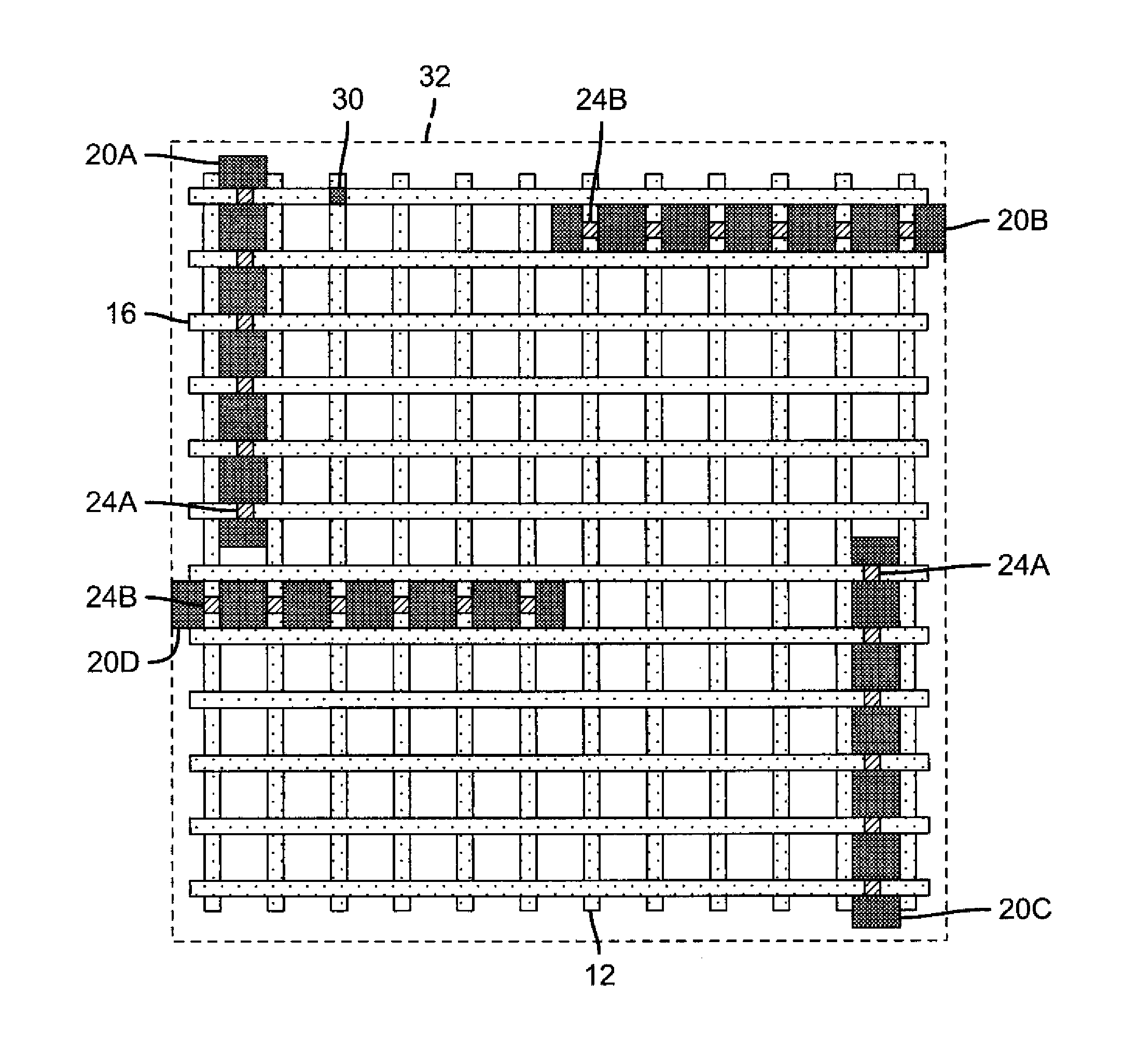
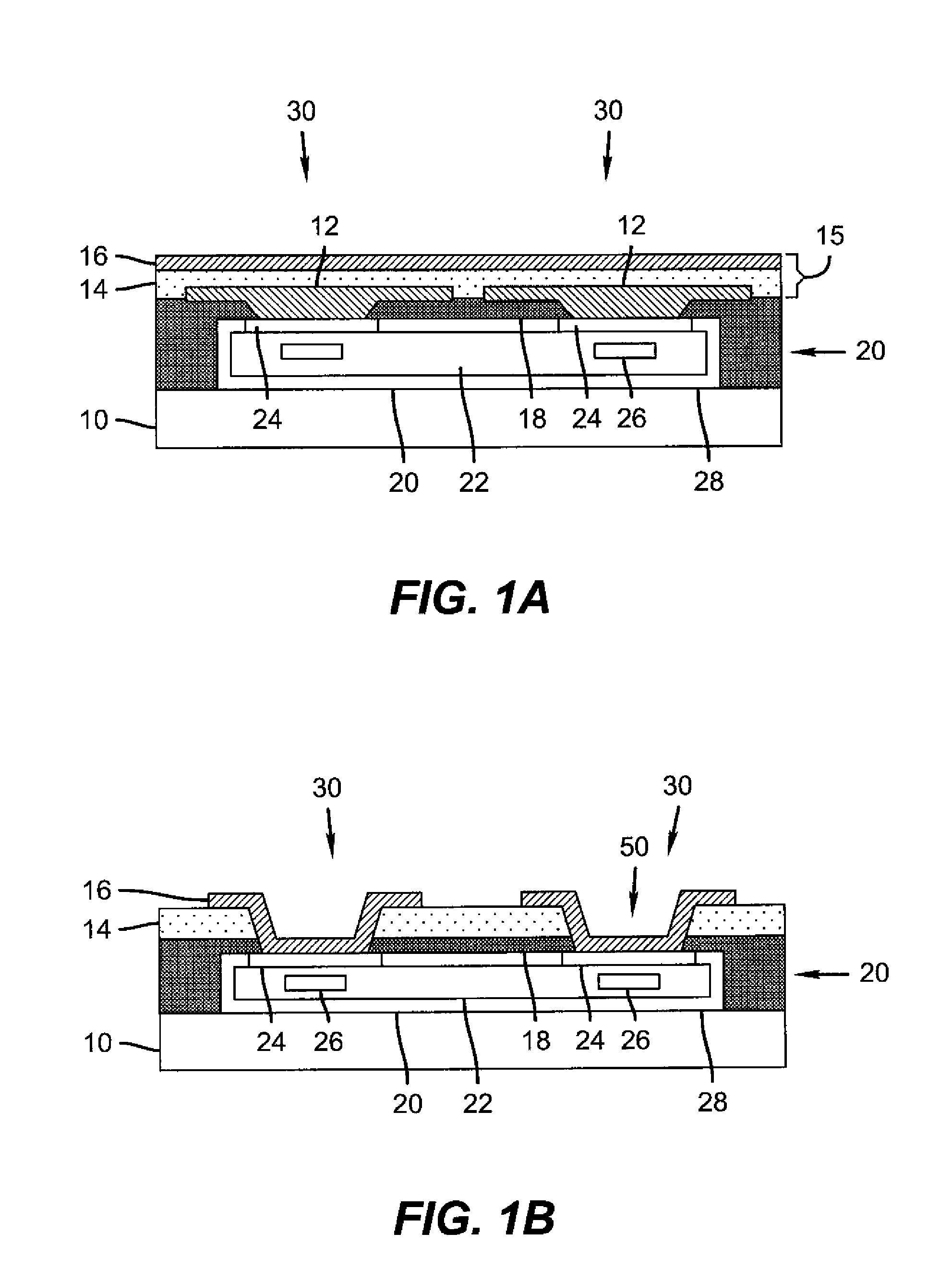
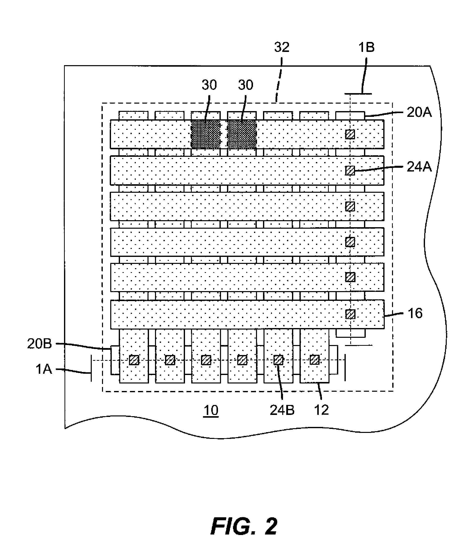
[0033]Referring to FIGS. 3 and 1A, in one embodiment of the present invention, a display device includes a substrate 10 and a first layer having an array of row electrodes 16 formed in rows across the substrate 10 in a first direction and a second layer having an array of column electrodes 12 formed in columns across the substrate 10 in a second direction different from the first direction. Pixel 30 locations are formed over the substrate 10, where the row and column electrodes 16, 12 overlap. One or more layers 14 of light-emitting material are formed between the row and column electrodes 16, 12 to form a two-dimensional array of pixels 30 in the pixel locations. A plurality of row driver chiplets 20A, 20C and a separate plurality of column driver chiplets 20B, 20D are distributed relative to the substrate 10, each row driver chiplet 20A, 20C exclusively connected to and controlling an independent set of row electrodes 16 and each column driver chiplet 20B, 20D exclusively connecte...


PUM


Abstract

A display device, including a substrate; a first layer having an array of row electrodes formed in rows across the substrate in a first direction and a second layer having an array of column electrodes formed in columns across the substrate in a second direction different from the first direction wherein the row and column electrodes overlap to form pixel locations; one or more layers of light-emitting material formed between the row and column electrodes to form a two-dimensional array of pixels, the pixels being located in the pixel locations; and a plurality of row driver chiplets and a separate plurality of column driver chiplets distributed relative to the two-dimensional array of pixels, each row driver chiplet exclusively connected to and controlling an independent set of row electrodes and each column driver chiplet exclusively connected to and controlling an independent set of column electrodes.

Description

CROSS-REFERENCE TO RELATED APPLICATION[0001]Reference is made to commonly-assigned U.S. patent application Ser. No. 12 / 191,462 filed Aug. 14, 2008, entitled “Display Device With Chiplets” by Ronald S. Cok et al, the disclosure of which is incorporated herein.FIELD OF THE INVENTION[0002]The present invention relates to display devices having a substrate with distributed, independent chiplets for controlling a pixel array.BACKGROUND OF THE INVENTION[0003]Flat-panel display devices are widely used in conjunction with computing devices, in portable devices, and for entertainment devices such as televisions. Such displays typically employ a plurality of pixels distributed over a substrate to display images. Each pixel incorporates several, differently colored light-emitting elements commonly referred to as sub-pixels, typically emitting red, green, and blue light, to represent each image element. As used herein, pixels and sub-pixels are not distinguished and refer to a single light-emit...

Claims


Application Information

Patent Timeline
Patent Type & Authority Applications(United States)
IPC IPC(8): G09G3/32
CPCG09G3/3208G09G3/3266G09G3/3275G09G2300/0426H01L27/3281G09G2310/0218G09G2310/0221G09G2320/0247H01L27/3255G09G2300/0465H10K59/129H10K59/17G09G3/32H10K59/00
Inventor COK, RONALD S.HAMER, JOHN W.
Owner GLOBAL OLED TECH
Why Eureka
Try Eureka