

Switch structure on sidewall of circuit board for electronic device and manufacturing method of the circuit board
a technology of switch structure and sidewall, which is applied in the direction of contact, printed circuit aspects, electrical apparatus construction details, etc., can solve the problem of limiting the volume of circuit boards and achieve the effect of reducing the space on the circuit boards
- Summary
- Abstract
- Description
- Claims
- Application Information
AI Technical Summary
Benefits of technology
Problems solved by technology
Method used
Image

Examples
first embodiment
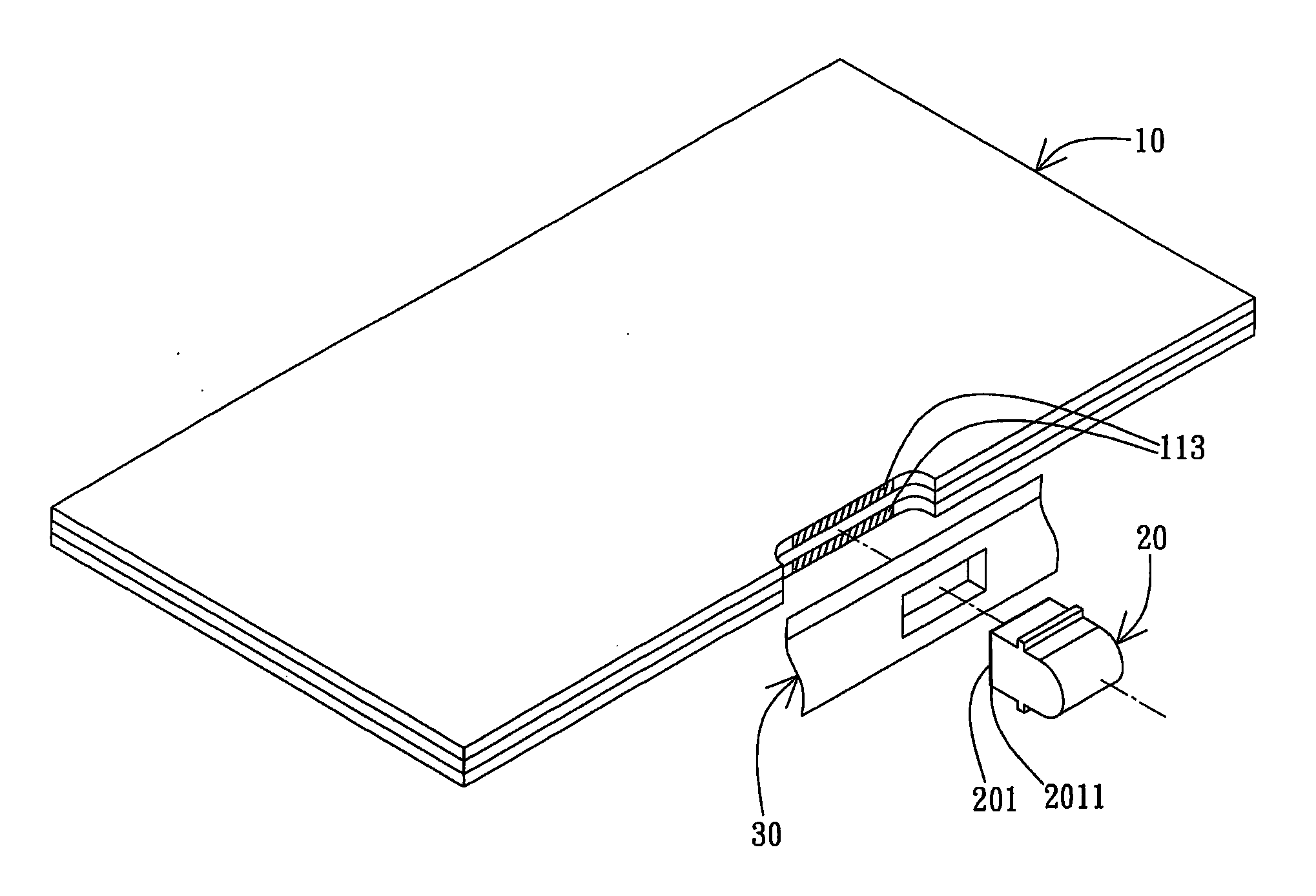
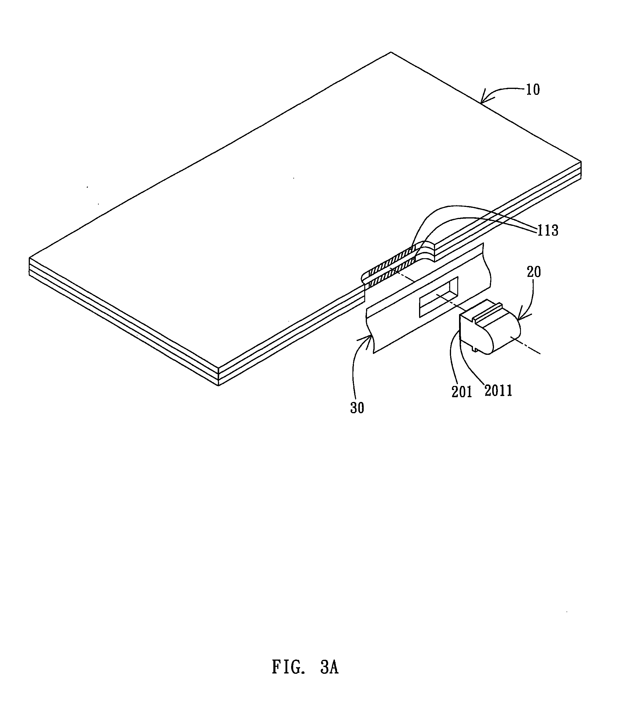
[0040]FIG. 3A shows an exploded view of a switch structure of an electronic device of the invention. As shown in FIG. 3A, the switch structure includes a circuit board 10, a movable unit 20 having a conducting part 201, and a housing 30. FIG. 3B shows a side view of the embodiment shown in FIG. 3A. As shown in FIG. 3B, the circuit board 10 includes a sidewall 11, a groove 111 formed on the sidewall 11, and two conductive portions 113 formed on the sidewall in the groove 111. The conductive portions 113 are electrically insulated from each other. For example, the conductive portions 113 can be conductive pins, leads, sections, layers, coatings, etc.
[0041]The conductive portions can be formed in various manners, so that the conductive portions are respectively formed on at least one of the sidewalls of circuit layers and electrically isolated from each other. For example, the conductive portions 113 can be formed in the groove 111. As shown in FIG. 4A, two conductive portions 113 can ...
fourth embodiment
[0044]In other embodiments, the movable unit can be disposed in a manner that the movable unit is electrically connected to one of the conductive portions. FIG. 6 shows an exploded view of the movable unit of the switch structure. As shown in FIG. 6, a portion of the movable unit 20 is electrically connected to one of the two conductive portions 113 while the other portion can be moved selectively. Pressing the movable unit 20 causes the two conductive portions 113 to become electrically connected. In this embodiment, the movable unit 20 is a body of non-conducting material with a conductive element 2011 disposed thereon. In such a case, pressing the body 20 causes the conductive element 2011 to contact the two conductive portions 113 so that the two conductive portions 113 become electrically connected, and the switch function is therefore achieved. However, in other embodiments, the movable unit 20 is a body of metal, electrically conductive rubber, graphite, or other conductive m...
fifth embodiment
[0045]Furthermore, in other embodiments, a metal plate can be disposed between the body and the conductive portions so that the conductive portions can become electrically connected through the metal plate. The advantage of using the metal plate is to provide the user with a button touch feeling due to the elasticity of the metal plate. FIG. 7A shows an exploded view of the movable unit of the switch structure. As shown in FIG. 7A, a portion of the metal plate 21 is electrically connected to one of the two conductive portions 113 while the other portion is fixed on the sidewall 11. FIG. 7B and FIG. 7C show schematic views of the movable unit 20 of FIG. 7A when the body is at the first position P1 and the second position P2 respectively. As shown in FIG. 7B and FIG. 7C, pressing the body 20 causes the metal plate 21 to deform and move from the first position P1 to the second position P2, so that the metal plate 21 contacts the other one of the two conductive portions 113 causing the ...
PUM
| Property | Measurement | Unit |
|---|---|---|
| Electrical conductivity | aaaaa | aaaaa |
| Shape | aaaaa | aaaaa |
| Electrical conductor | aaaaa | aaaaa |
Abstract
Description
Claims
Application Information