Electronic parts, and method for arranging shielding case and chip parts

Inactive Publication Date: 2010-08-26
LENOVO INNOVATIONS LTD HONG KONG
View PDF3 Cites 1 Cited by
  • Summary
  • Abstract
  • Description
  • Claims
  • Application Information

AI Technical Summary

Benefits of technology

[0013]Accordingly, in view of the foregoing problem, an object of the present invention is to provide an electronic part, in which an opening is provided on a top face of a shielding case, having minimized clearance between the shielding case and chip parts so as to reduce the thickness of a device, and a method for arranging the shielding case and the chip parts to form such electronic part.
[0022]As described above, the present invention includes locating at regular intervals on a substrate the plurality of chip parts each having on a respective end portion a ground terminal and an electrode terminal that supplies a voltage source, such that the respective ground terminals are aligned, and electrically connecting the ground terminal and the electrode terminal to a ground terminal land and an electrode terminal land of the substrate respectively; forming an opening on the shielding case through which a resin is to be provided for securing strength of the respective electrical connection points of the ground terminal land and the electrode terminal land of the substrate with the ground terminal and the electrode terminal of the chip parts; and forming the opening such that an edge of the opening becomes parallel to the ground terminal of the respective chip parts, and such that upon being warped the opening edge and the ground terminal of the respective chip parts contact each other, and such that upon being warped a portion of the chip parts other than a grounding part opposes the opening without contacting the edge of the opening, and therefore enables minimizing a clearance between the shielding case and chip parts so as to reduce the thickness of a device, in the case where an opening is provided on a top face of a shielding case for providing a resin therethrough to thereby secure strength of the terminal portion of the chip parts.
[0023]The present invention also enables further reducing the risk that the shielding case contacts the peripheral parts.
[0024]Further, the present invention allows securing diversity in arranging the layout of the plurality of chip parts, in the case where the ground terminals of the plurality of chip parts cannot be linearly aligned.

Problems solved by technology

Recently, it is becoming more difficult to secure the clearance between the shielding case and the chip parts enclosed therein, under the restriction imposed by requirement for reducing the thickness of a device in which the electronic part is to be implemented.
With such structure, in the case where bending force is applied from outside to the top face of the shielding case, stress is concentrated at the opening on the top face of the shielding to thereby warp the edge of the opening, which may bring the shielding case and the chip parts in the shielding case into contact and thus causing short circuit and resultant malfunctions such as erroneous action and abnormal heat generation.
However, since the openings are made small from the viewpoint of strength of the outer case, shielding effect against electromagnetic interference, and intrusion of a foreign substance, such openings are inappropriate for providing the resin therethrough, for securing the drop strength of the terminal portion of the chip parts as stated above.
However, such technique is not intended for minimizing the distance between the shielding case and the chip parts thereby reducing the thickness of the device, in the electronic part encapsulated with the resin for securing the drop strength of the terminal portion of the chip parts, as stated above.

Method used


Image

  • Electronic parts, and method for arranging shielding case and chip parts
  • Electronic parts, and method for arranging shielding case and chip parts
  • Electronic parts, and method for arranging shielding case and chip parts

Examples


example 1

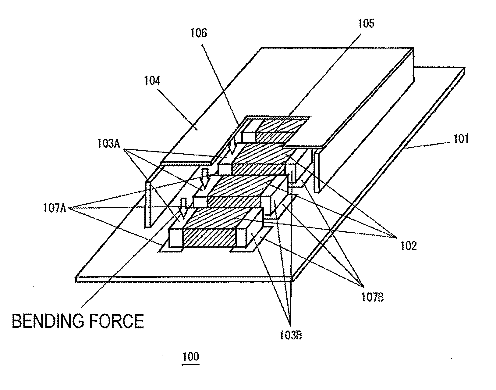
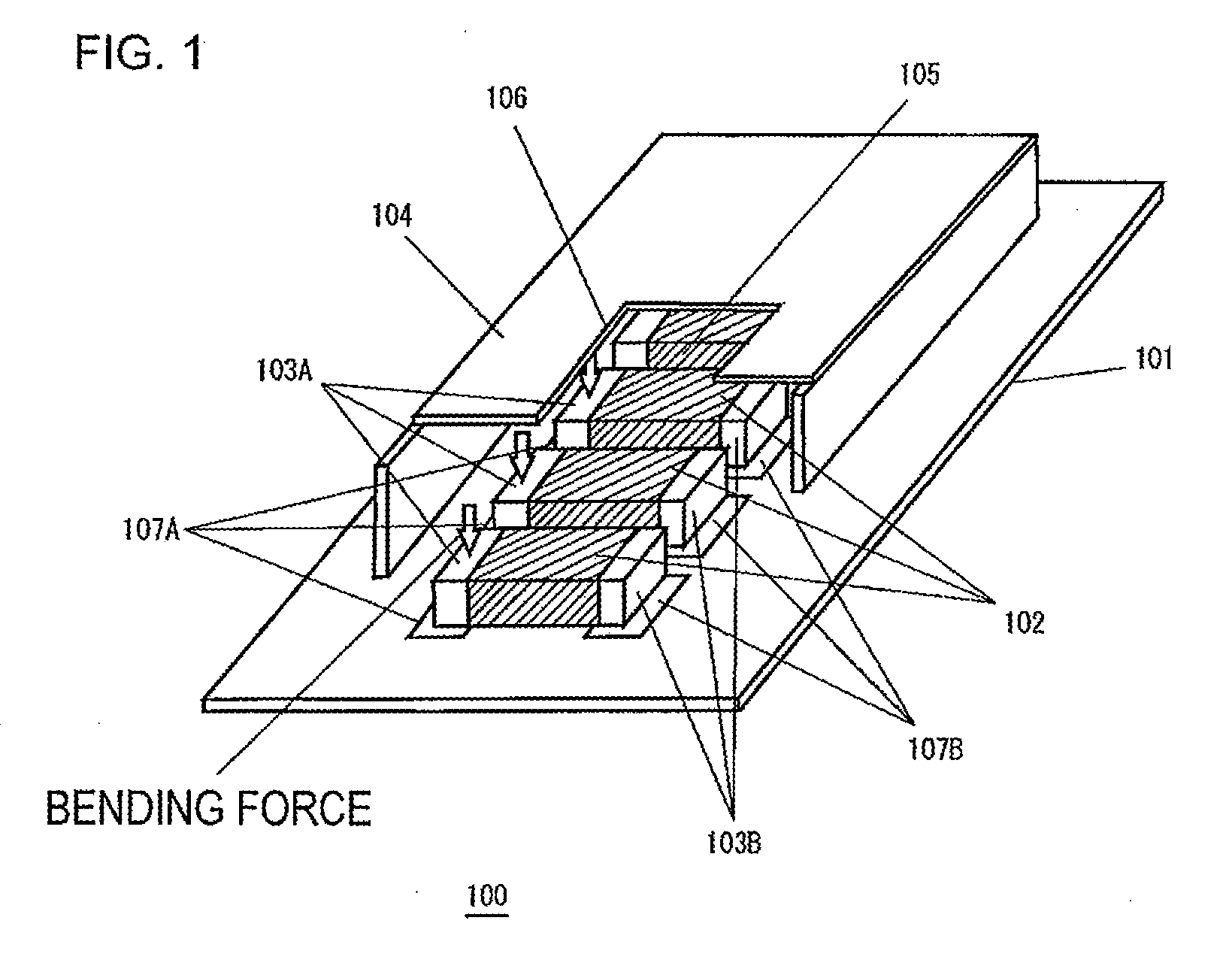
[0045]FIGS. 5(a) and 5(b) are side views of the electronic part 100, for explaining comparison of the height of the chip parts 102 and peripheral parts shown in FIG. 1. In FIG. 5(a), bending force is applied to the top face of the shielding case 104, and the edge 106 of the opening 105 is warped so as to contact the ground terminal 103A of the chip part 102. Under such state, in the case where the peripheral parts 201 are located around the chip parts 102, the clearance between the peripheral parts 201 and the shielding case 104 thus warped is denoted as g1.

[0046]Upon comparing the height of the peripheral parts 201 and that of the chip part 102, in the case where the peripheral parts 201 and the chip part 102 are of the same height, the clearance g1 becomes small and hence the shielding case 104 and the peripheral parts 201 are prone to contact each other.

[0047]Accordingly, the peripheral parts 201 are mounted such that the height thereof becomes lower than that of the chip part 10...

example 2

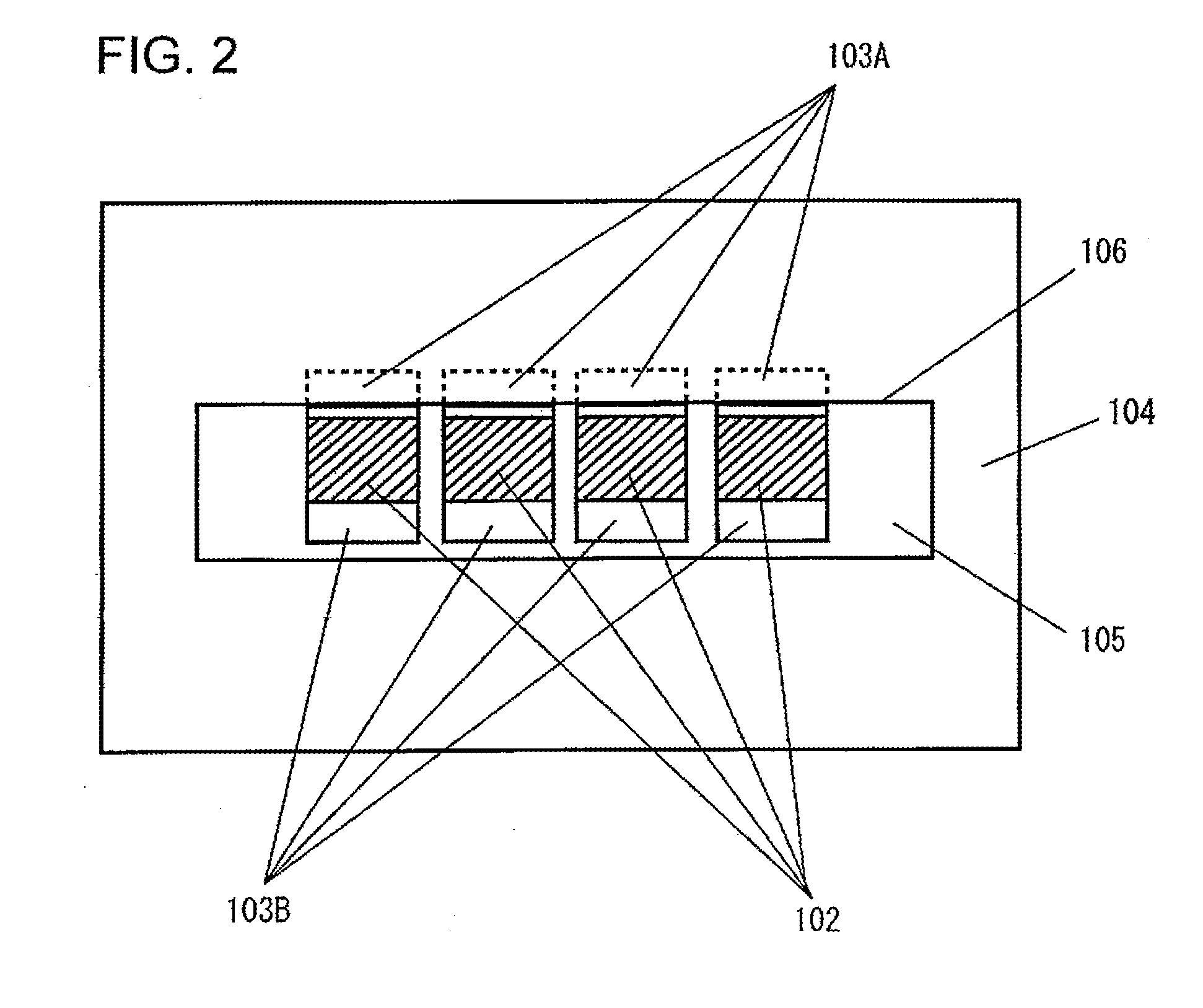
[0049]FIG. 6 is a modification of FIG. 2, and a plan view of a layout of the opening 105 of the shielding case 104 and the plurality of chip parts 102 shown in FIG. 1, from above. In comparison with FIG. 2, a difference in FIG. 6 is that the ground terminal 103A of a plurality of chip parts 102-1 are linearly aligned so as to overlap a portion of the opening edge 106 opposite to the portion thereof on the side the ground terminal 103A of plurality of chip parts 102. The portion of the plurality of chip parts 102-1 other than the portion overlapping with the shielding case 104 is seen through the opening 105, and the chip parts 102-1 are located such that the respective electrode terminals 103B do not overlap with the shielding case 104, in other words such that the respective electrode terminals 103B do not contact the shielding case 104 when the opening edge 106 is warped.

[0050]The present invention allows, therefore, securing diversity in designing the layout of the plurality of c...

example 3

[0051]FIG. 7 is another modification of FIG. 2, and a plan view of a layout of the opening 105 of the shielding case 104 and the plurality of chip parts 102 shown in FIG. 1, from above. In comparison with FIG. 2, a difference in FIG. 7 is that the respective ground terminals 103A of a plurality of chip parts 102-2 are linearly aligned so as to overlap a portion of the opening edge 106 orthogonal to the portion thereof along the plurality of chip parts 102. The portion of the plurality of chip parts 102-2 other than the portion overlapping with the shielding case 104 faces the opening 105 so as to be seen therethrough, and the chip parts 102-2 are located such that the respective electrode terminals 103B do not overlap with the shielding case 104, in other words such that the respective electrode terminals 103B do not contact the shielding case 104 when the opening edge 106 is warped.

[0052]The present invention allows, therefore, securing diversity in designing the layout of the plur...


PUM


Abstract

An electronic part (100) that shields parts on a substrate (101) includes a plurality of chip parts (102) each having on a respective end portion a ground terminal (103A) and an electrode terminal (103B) that supplies a voltage source, and located at regular intervals on the substrate with the respective ground terminals aligned, the ground terminal and the electrode terminal being electrically connected to a ground terminal land (107A) and an electrode terminal land (107B) of the substrate respectively; and a shielding case (104) that shields the plurality of chip parts and includes an opening (105) through which a resin is to be provided for securing strength of the respective electrical connection points of the ground terminal land and the electrode terminal land of the substrate with the ground terminal and the electrode terminal of the chip parts; the opening being formed such that an edge (106) of the opening becomes parallel to the ground terminal of the respective chip parts, and such that upon being warped the opening edge and the ground terminal of the respective chip parts contact each other, and such that upon being a portion of said chip parts other than a grounding part opposes the opening without contacting the edge of the opening.

Description

TECHNICAL FIELD[0001]The present invention relates to an electronic part including chip parts shielded in a shielding case. More particularly, the present invention relates to an electronic part in which the shielding case is encapsulated with a resin through an opening on a top face thereof for securing drop strength of a terminal portion of the chip parts, with minimized clearance between the shielding case and the chip parts, and to a method for arranging the shielding case and the chip parts to form such electronic part.BACKGROUND ART[0002]On an electronic part, generally, chip parts including a semiconductor IC and so forth are enclosed in a shielding case, for assuring electromagnetic compatibility (EMC). Also, in order to avoid short circuit caused by contact of the shielding case and a power source of the chip parts in the shielding case, the shielding case is made sufficiently high to thereby secure a clearance between the shielding case and the chip parts.[0003]Recently, i...

Claims


Application Information

Patent Timeline
IPC IPC(8): H01L23/552H01L21/50
CPCH05K9/0026
Inventor OGURI, SHINJI
Owner LENOVO INNOVATIONS LTD HONG KONG
Why Eureka
Try Eureka