Method for manufacturing semiconductor device, semiconductor device and molding die

a semiconductor device and molding die technology, applied in the direction of manufacturing tools, applications, drawing profiling tools, etc., can solve the problems of deterioration in moisture resistance, inability to obtain predetermined breakdown voltage, etc., and achieve the effect of reducing resin pressure and reducing the tilt of the island 12

Active Publication Date: 2010-09-02
SEMICON COMPONENTS IND LLC
View PDF1 Cites 13 Cited by
  • Summary
  • Abstract
  • Description
  • Claims
  • Application Information

AI Technical Summary

Benefits of technology

[0019]A method for manufacturing a semiconductor device according to the present invention includes the steps of: preparing a molding die formed of a first die and a second die, the molding die having at least a plurality of cavities connected in series through runners from a pod; disposing a lead frame in the molding die in a state where a mounting part having at least an island and leads having one ends connected to the island is disposed in each of the cavities, where a semiconductor element is fixed on one side of the island and where the leads and the semiconductor element are electrically connected to each other through thin metal wires; and injecting a molten resin into at least the plurality of cavities through the runners from the pod and injecting the molten resin into each of the cavities including a space between the other side of the island and the first die, wherein a position of an outlet of the molten resin in the cavity is set closer to one side than a position of an inlet of the molten resin in the cavity is, thereby preventing displacement of the island near the outlet, the inner lead near the outlet or the thin metal wires near the outlet.
[0020]Furthermore, a method for manufacturing a semiconductor device according to the present invention includes the steps of: preparing a molding die formed of a first die and a second die, the molding die having at least a plurality of cavities connected in series through runners from a pod; disposing a lead frame in the molding die in a state where a mounting part is disposed in each of the cavities, the mounting part having a rectangular island with first and second sides facing each other and third and fourth sides facing each other, holding leads provided on the first and second sides close to an inlet and an outlet of the cavity, and a plurality of leads having one ends disposed on the third and fourth sides intersecting with the first side, where a semiconductor element is fixed on one side of the island, and where the leads and the semiconductor element are electrically connected to each other through thin metal wires; and injecting a molten resin into at least the plurality of cavities through the runners from the pod and injecting the molten resin into each of the cavities including a space between the other surface of the island and the first die, wherein a position of an outlet of the molten resin in the cavity is set closer to one side than a position of an inlet of the molten resin in the cavity is, thereby preventing displacement of the island near the outlet, the inner lead near the outlet or the thin metal wires near the outlet.
[0021]With reference to FIGS. 6A to 6C, the resin in the cavity 36A subsequently fills the space between the island 12 and the upper die. In this event, since there is more resin near the outlet P1, a downward force acts on the island 12. However, by setting the position of the outlet P1 above the island, more specifically, further above the position of the gate P2, an amount of the resin applying a pressure can be actively sent to the next cavity. Thus, the resin pressure is reduced for the amount of the resin sent. Consequently, the tilt of the island 12 can be reduced.

Problems solved by technology

However, the above sealing resin injection method has a problem that the island 206 is moved by an injection pressure of the resin injected into the cavity 200A.
Thus, there is a possibility that a predetermined breakdown voltage cannot be obtained.
This also leads to deterioration in moisture resistance.

Method used


Image

  • Method for manufacturing semiconductor device, semiconductor device and molding die
  • Method for manufacturing semiconductor device, semiconductor device and molding die
  • Method for manufacturing semiconductor device, semiconductor device and molding die

Examples


embodiment 1

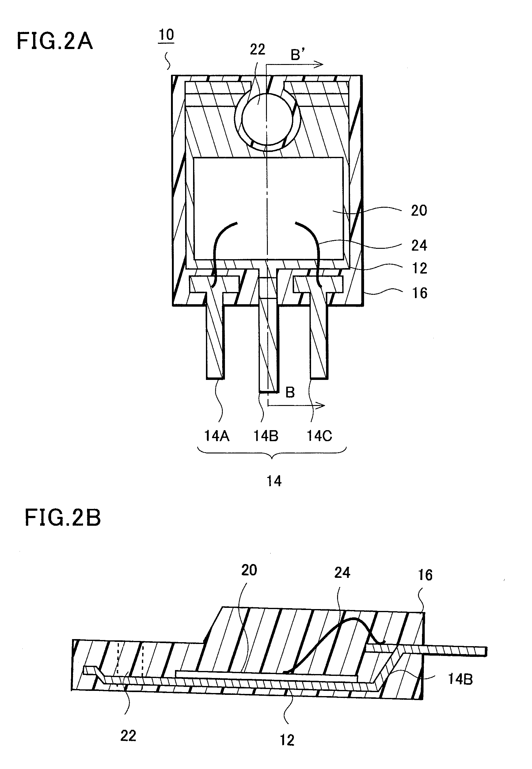
[0044]With reference to FIG. 2, Embodiment 1 will be described. FIG. 2A is a plan view showing a semiconductor device 10 and FIG. 2B is a cross-sectional view taken along the line B-B′ in FIG. 2A.

[0045]The semiconductor device 10 is a discrete transistor, in which a back surface of an island 12 is covered with a resin, and is, for example, a 3-terminal package or a package such as TO220. This semiconductor device 10 mainly includes: the island 12; a semiconductor element 20 mounted on an upper surface of the island 12; a lead 14 which functions as an external connection terminal; and a sealing resin 16 integrally covering and mechanically supporting those described above. A lead 14B is extended integrally with the island 12 and serves as an electrode at a current outflow side (or inflow side). One of leads 14A and 14C serves as a control electrode and the other serves as an electrode at a current inflow side (or outflow side). Specifically, the semiconductor element 20 is a BIP Tr, ...

embodiment 2

[0052]With reference to FIGS. 3A to 6C, a method for manufacturing a semiconductor device will be described next.

[0053]With reference to FIG. 3A, an external shape of a lead frame 50 is a strip shape. Inside a frame-shaped outer frame 52, plural units 56 (mounting part) are formed in a matrix pattern.

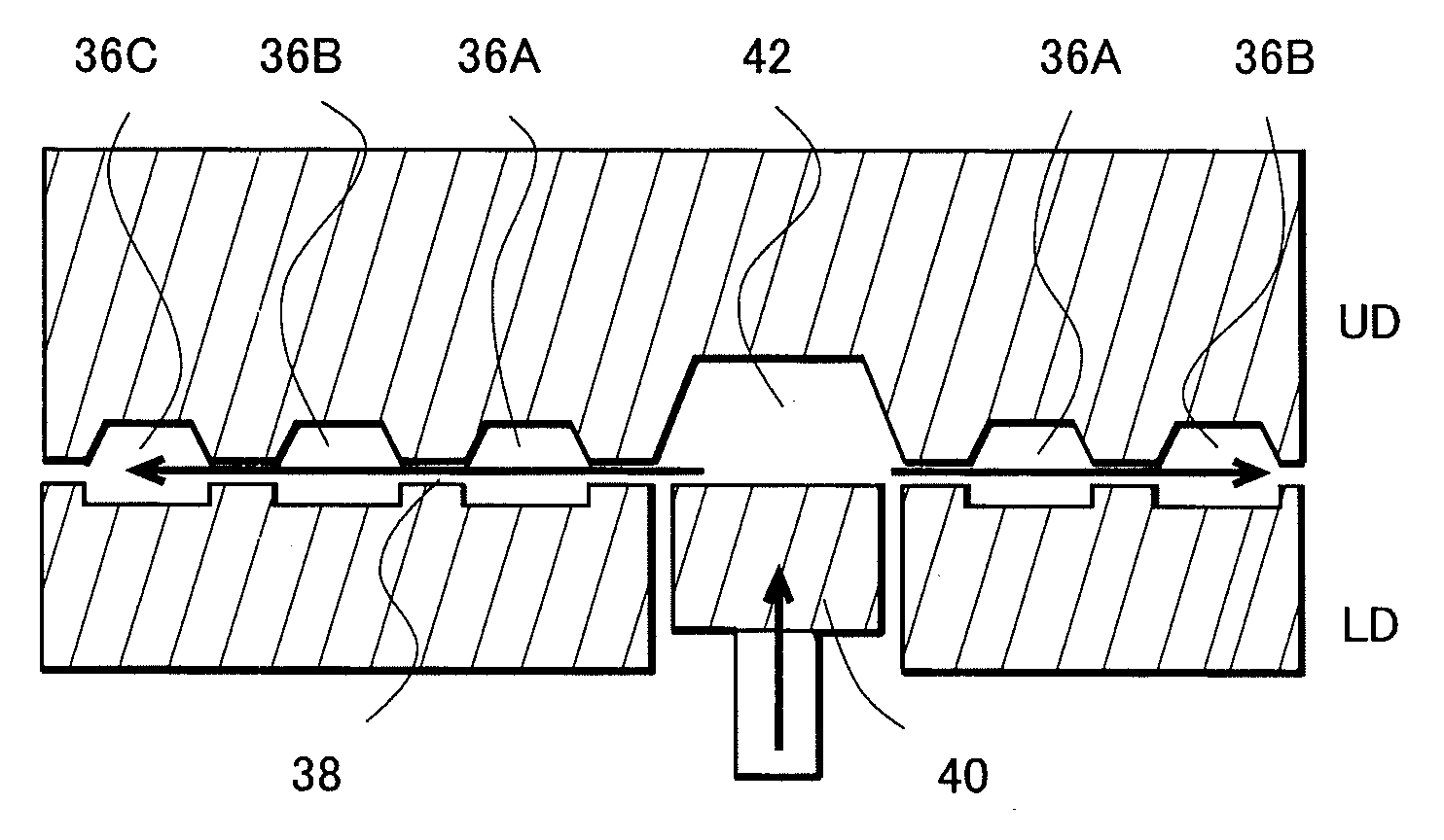
[0054]FIG. 3B is a partially enlarged plan view of FIG. 3A. Here, tie bars 58 are extended so as to connect upper and lower outer frames 52. On the page space, the units 56A to 56D are arranged in a line on the left side and connected to each other by the tie bar 58, and the units 56E to 56H are arranged in a line on the right side and connected to each other by the tie bar 58.

[0055]Each of the units includes an island 12 and leads 14A to 14C. Moreover, one ends of the leads 14A and 14C are set close to the island 12 and the lead 14B is extended integrally with the island 12. Furthermore, intermediate portions and end portions of the leads 14A to 14C in the unit 56A are connected with t...

embodiment 3

[0077]Subsequently, with reference to FIGS. 8 to 12, description will be given of the fact that the present invention can also be applied to an IC. FIG. 8A shows a semiconductor device without an insulating resin. FIG. 8B is a cross-sectional view of the semiconductor device sealed with an insulating resin 106. The semiconductor device shown in FIGS. 8A and 8B includes: a rectangular island 100; lead groups 101 . . . , 101 . . . having one ends adjacent to left and right sides of the island 100; upper and lower suspension leads 102 extended outward from upper and lower sides of the island 100 and integrally holding the island; an IC chip 103 fixed on the island 100; and thin metal wires 105 electrically connecting bonding pads 104 on the chip 103 to the leads 101. The entire device is covered with the insulating resin 106 except for a portion corresponding to outer leads of the leads. Here, although two holding leads 102 are shown in FIG. 8, there may be at least one holding lead. N...


PUM

PropertyMeasurementUnit
currentaaaaaaaaaa
thicknessaaaaaaaaaa
thicknessaaaaaaaaaa

Abstract

Provided is a method for manufacturing a semiconductor device in which movement of an island in resin sealing is prevented. A molding die includes an upper die and a lower die. The upper and lower dies are fitted together to form cavities and runners. In the lower die, a pod is provided. After heating and melting of a tablet made of a solid resin and housed in the pod, the melted sealing resin is pressurized by a plunger, and is supplied to each of the cavities. Specifically, a liquid sealing resin is supplied from the pod to the cavities, sequentially, from the upstream of the flow of the sealing resin supplied from the pod. The cavities communicate with each other through the runners. Furthermore, the runners through which the cavities communicate are provided to be tilted with respect to a path for supplying the sealing resin.

Description

[0001]This application claims priority from Japanese Patent Application Number JP2009-46355 filed on Feb. 27, 2009, and Japanese Patent Application Number JP2009-46356 filed on Feb. 27, 2009, the contents of which are incorporated herein by reference in their entirety.BACKGROUND OF THE INVENTION[0002]1. Field of the Invention[0003]The present invention relates to a method for manufacturing a semiconductor device, a semiconductor device and a molding die.[0004]2. Description of the Related Art[0005]A process for manufacturing a semiconductor device is classified broadly into a pre-process for mounting desired elements on a semiconductor wafer and a post-process for packaging semiconductor elements obtained by dividing the semiconductor wafer. The post-process includes a step of sealing the semiconductor elements with a resin.[0006]This sealing step will be described with reference to FIGS. 7A to 7C. In the sealing step, disruption of a balance of resin pressure due to providing a res...

Claims


Application Information

Patent Timeline
Patent Type & Authority Applications(United States)
IPC IPC(8): H01L23/495H01L21/56B29C45/14
CPCH01L21/565H01L2924/1305H01L24/97H01L2224/48091H01L2224/48247H01L2224/49171H01L2224/97H01L2924/01013H01L2924/01029H01L2924/01033H01L2924/01047H01L2924/01079H01L2924/01082H01L2924/13055H01L2924/13091H01L2924/14H01L23/49562H01L2924/1306H01L2224/48472H01L2924/12041H01L2924/01322H01L2924/01006H01L2924/01005H01L24/49H01L24/48H01L2224/85H01L2924/00014H01L2924/00H01L24/45H01L2224/05554H01L2224/451H01L2224/45124H01L2224/45144H01L2224/45147H01L2924/181
Inventor YOSHIBA, SHIGEHARUFUKUDA, HIROKAZU
Owner SEMICON COMPONENTS IND LLC
Why Eureka
Try Eureka