

Hermetic packaging of integrated circuit components
a technology of integrated circuit components and packaging, which is applied in the field of integrated circuits, can solve the problems of difficult and expensive packaging of such devices, significantly degrading electrical performance, etc., and achieves the effect of reducing the handling of individual chips and reducing or eliminating the labor of bonding i/o
- Summary
- Abstract
- Description
- Claims
- Application Information
AI Technical Summary
Benefits of technology
Problems solved by technology
Method used
Image

Examples
Embodiment Construction
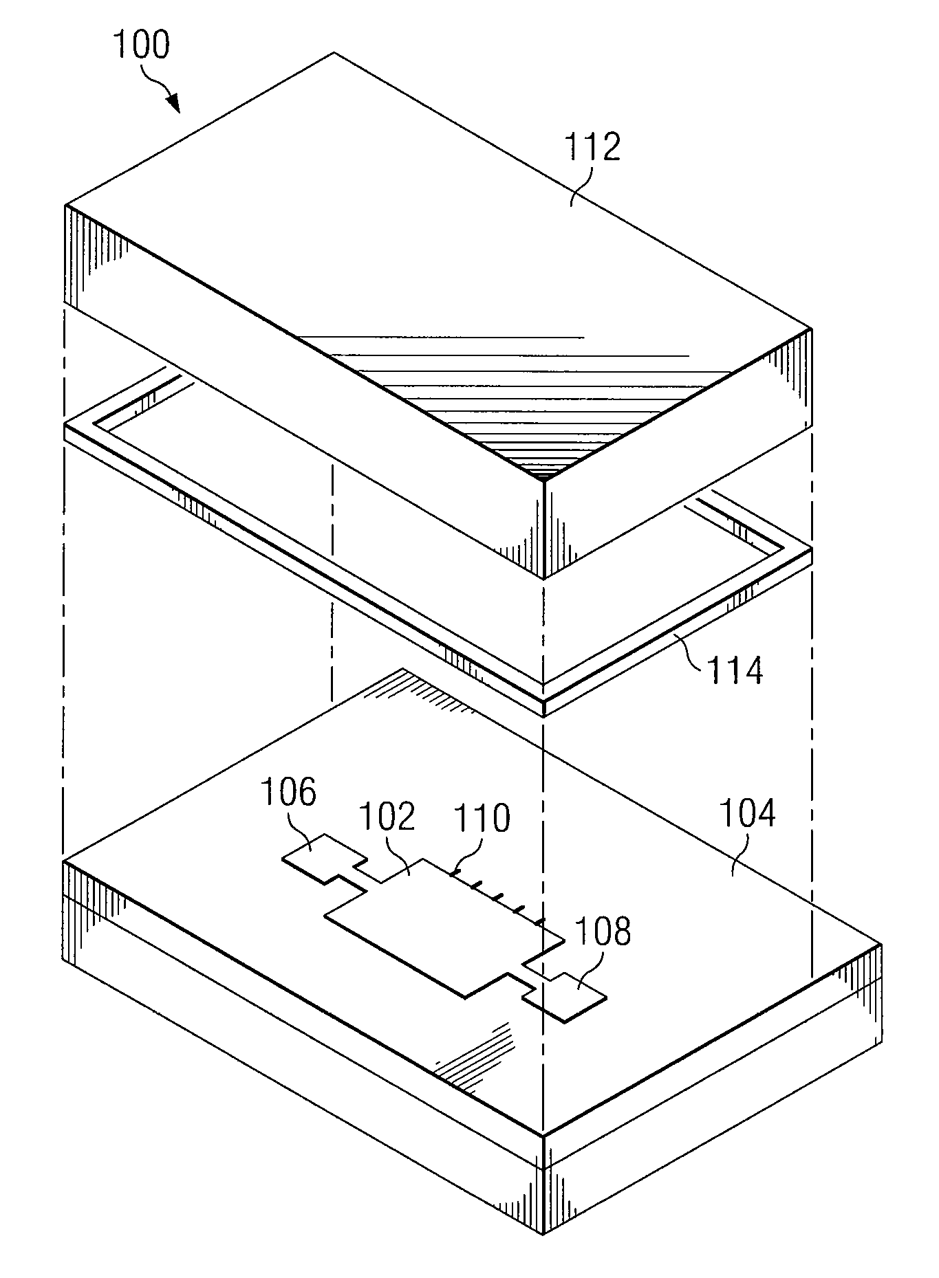
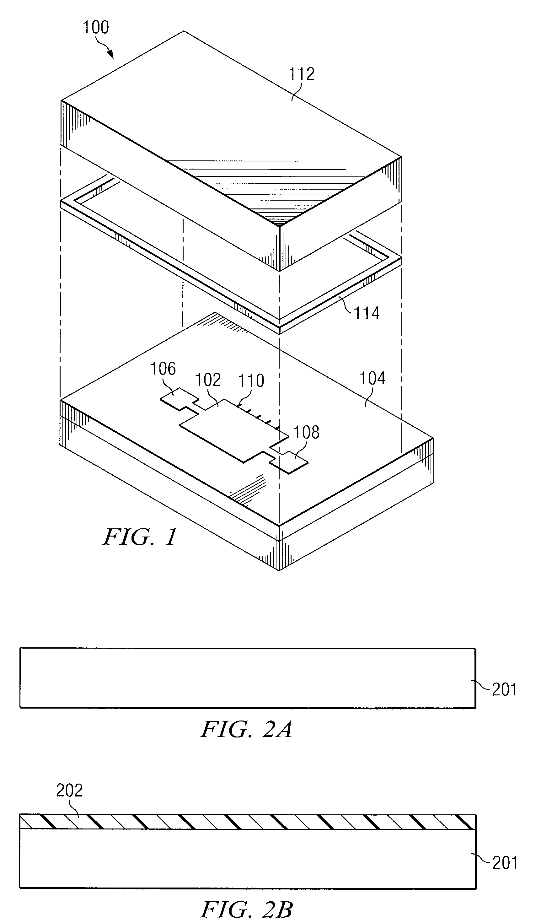
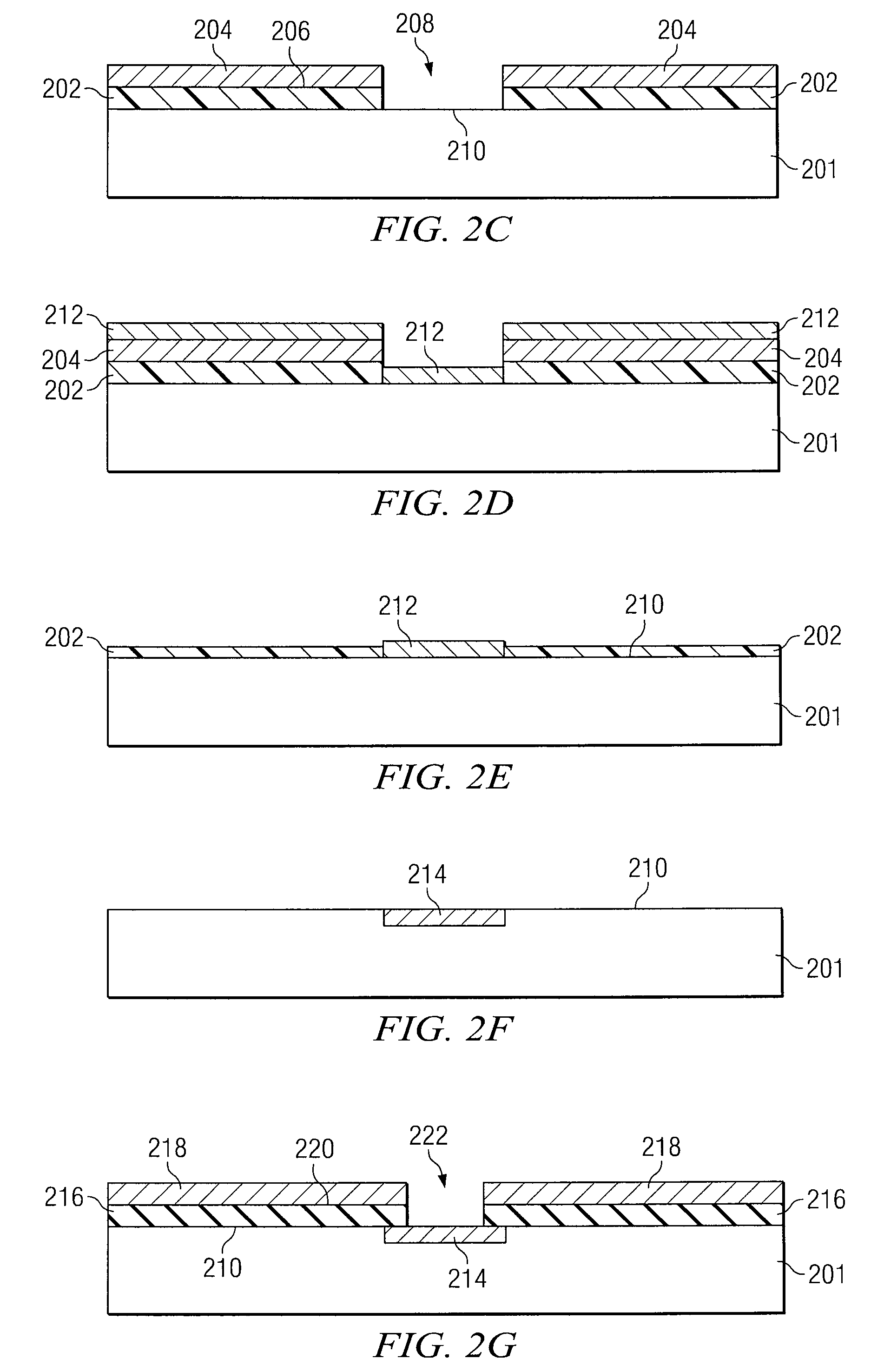
[0006]According to one embodiment of the present invention, a method for forming an integrated circuit includes transforming at least a portion of a first substrate layer to form a conductive region within the first substrate layer. An integrated circuit device is provided proximate an outer surface of the first substrate layer. The integrated circuit device transmits or receives electrical signals through the conductive region. A second substrate layer is disposed proximate to the outer surface of the first substrate layer to enclose the integrated circuit device in a hermetic environment. Historically, integrated circuits are fabricated on silicon wafers, diced into individual circuit chips, and each is then individually mounted inside a package. The I / O's for the chips are bonded to the I / O's of the package. Hermiticity depends on the hermiticity of the package and its I / O's. Conventional hermitic packaging can be many times more expensive than the IC chip itself. Depending on th...
PUM
 Abstract
Description
Claims
Application Information