Semiconductor apparatus packaging structure, semiconductor apparatus packaging method, and embossed tape

a technology of semiconductor apparatus and packaging structure, which is applied in the direction of packaging goods type, transportation and packaging, containers, etc., can solve the problems of insufficient protection measures, high probability of leakage, and inability to use spacer tape, and achieve the effect of convenient height adjustmen

Active Publication Date: 2010-09-16
TAIWAN SEMICON MFG CO LTD
View PDF10 Cites 20 Cited by
  • Summary
  • Abstract
  • Description
  • Claims
  • Application Information

AI Technical Summary

Benefits of technology

[0022]Note that the spacer tape 700 (see Patent Literature 2) is intended for use in the TAB tape 750 on which semiconductor chips have not yet been mounted. In view of this, measures are insufficiently taken to protect, during shipping and transportation, a TAB tape on which the semiconductor chips are mounted. A vibration is caused during shipping and transportation, and it is therefore necessary to cause the protruding parts 702 to have a sufficient height so as to prevent damage to at least the semiconductor chips. As far as a protruding part which has a low height is concerned, Patent Literature 3 discloses a laminate spacer tape for use in (i) a circuit production process and (ii) a circuit tape on which semiconductor chips are mounted and protruding parts which have a low height are provided. This laminate spacer tape is intended for use from a state of a raw tape on which a circuit has not yet been configured. This allows the protruding parts to have a low height.
[0049]Therefore, it is possible for the embossed tape to function as an embossed tape for shipping and transportation, that is, to serve as cushioning against a semiconductor apparatus. Note that it is easy to thermally deform the embossed tape so as to carry out embossing because the embossed tape is made of a monolayer. Note also that the protruding parts are easily height-adjustable. This brings about an effect of realizing packaging of a semiconductor apparatus in a desired winding length while sufficiently securing protection of the semiconductor apparatus with which the embossed tape is wound on a reel.

Problems solved by technology

However, there is a problem that it is impossible for the spacer tape 600 (see Patent Literature 1) and the spacer tape 700 (see Patent Literature 2) to achieve winding of a TAB tape in a recently-demanded length while sufficiently securing protection of the TAB tape during shipping and transportation.
In view of this, measures are insufficiently taken to protect, during shipping and transportation, a TAB tape on which the semiconductor chips are mounted.
In view of this, in a case where dusting occurs because the spacer tape is rubbed, a defect caused by leak is highly likely to occur.

Method used


Image

  • Semiconductor apparatus packaging structure, semiconductor apparatus packaging method, and embossed tape
  • Semiconductor apparatus packaging structure, semiconductor apparatus packaging method, and embossed tape
  • Semiconductor apparatus packaging structure, semiconductor apparatus packaging method, and embossed tape

Examples


example 1

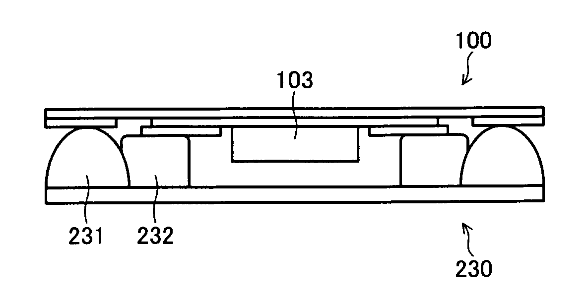
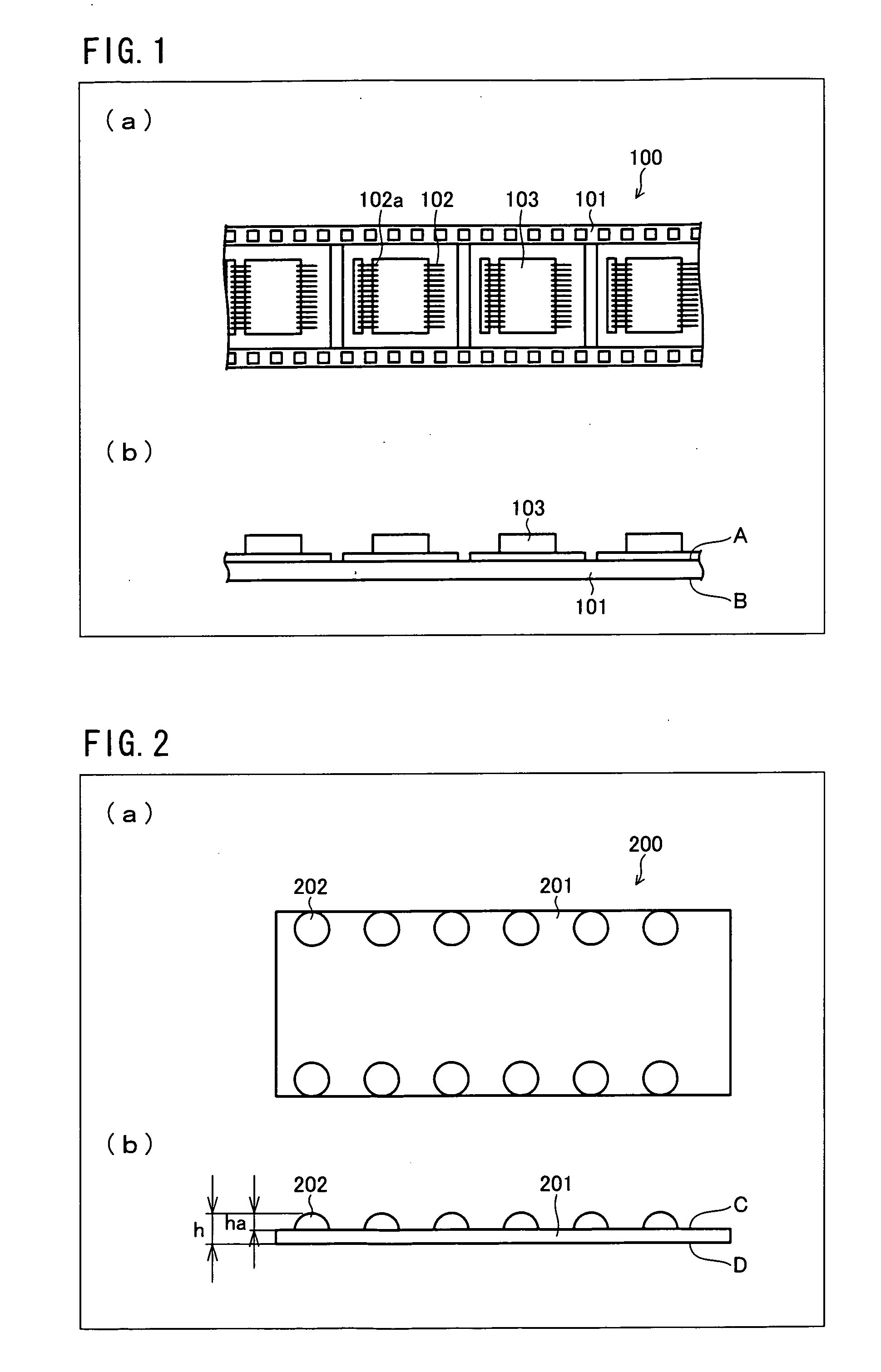
[0147]It was tested how long the TAB tape 100 (a thickness of the film 101: 0.04 mm, a thickness of the semiconductor chip 103: 0.625 mm) (see FIG. 1) can be wound, in accordance with a total thickness of the embossed tape 200 (a thickness of the film 201: 0.125 mm) (see FIG. 2), on the reel 310 which has a size of Φ 405 mm.

[0148]Note that, according to the TAB tape 100, a lead tape is actually provided at each of a front end part and a back end part of the TAB tape 100 so that workability is improved in a production process. FIG. 15 illustrates the TAB tape 100 which has the lead tapes at its front end part and back end part. The lead tape, provided at the front end part of the TAB tape 100, is caused to, for example, pass through a slit provided on the core section 311 of the reel 310. The lead tape is thus used to cause the TAB tape 100 to be fixed at the start of winding of the TAB tape 100. The lead tape, provided at the back end part of the TAB tape 100 is extended to a tape u...

example 2

[0157]In a case where the TAB tape 100 and the embossed tape 200 are wound while overlapping each other, a gap g is secured between the semiconductor chip 103 and the embossed tape 200 (see FIG. 19). However, a warp(s) in the TAB tape 100 and / or in the embossed tape 200 may cause the embossed tape 200 to be rubbed due to a contact between the semiconductor chip 103 and the embossed tape 200.

[0158]In view of the circumstances, it was checked, in accordance with the gap between the semiconductor chip 103 and the embossed tape 200, whether or not the embossed tape 200 was rubbed. FIG. 21 shows a distance of the gap which varies depending on a combination of (i) a total thickness and a real height of the embossed tape 200 and (ii) a thickness of the semiconductor chip 103. The semiconductor chips 103 which have respective thicknesses of 0.4 mm, 0.625 mm, and 0.725 mm were used. The embossed tapes 200 which have respective total thicknesses of 0.8 mm to 1.2 mm in increments of 0.1 mm wer...


PUM

PropertyMeasurementUnit
thicknessaaaaaaaaaa
thicknessaaaaaaaaaa
tensionaaaaaaaaaa

Abstract

A TAB tape (100) packaging structure in which (i) the TAB tape (100) including a plurality of semiconductor chips (103) which are fixed, on a film (101) on which wiring patterns are repeatedly provided and (ii) an embossed tape (200) which is electroconductive and has embossed parts (202) which are sequentially provided on a first surface of and in a longitudinal direction of a film (201) are wound on a reel which is electroconductive is arranged such that the TAB tape (100) and the embossed tape (200) are wound on the reel, while (i) a first surface of the film (101) on which surface the plurality of semiconductor chips (103) are fixed and (ii) the first surface of the film (201) on which surface the embossed parts (202) protrude are overlapping and facing each other, and the embossed tape (200) has a total thickness of not less than (t+0.4) mm and not more than 1.1 mm in a case where each of the plurality of semiconductor chips (103) has a thickness of t (0.2≦t≦0.625) mm and the film (201) has a substantial thickness of 0.125 mm. This realizes packaging of a TAB tape in a desired winding length while sufficiently securing protection of the TAB tape during shipping and transportation.

Description

TECHNICAL FIELD[0001]The present invention relates to a semiconductor apparatus packaging structure, and a semiconductor apparatus packaging method, each of which allows a semiconductor apparatus mounted on a tape to be shipped and transported in a state where the semiconductor apparatus, together with the embossed tape, has been wound on a reel, and to an embossed tape for use in packaging the semiconductor apparatus.BACKGROUND ART[0002]Drivers ICs or drivers LSI for a liquid crystal display are mounted in a structure of TCP (Tape Carrier Package) or COF (Chip on Film). Such a structure is referred to as a TAB (Tape Automated Bonding) tape. A film mounting IC or LSI is used as a semiconductor chip mounted on the TAP tape.[0003]According to such a TAB tape, a circuit is provided on a tape-like film on which the semiconductor chips are mounted and wiring patterns are provided. The TAB tape is therefore entirely thin and can be bent freely to some extent in any place. Therefore, the T...

Claims


Application Information

Patent Timeline
Patent Type & Authority Applications(United States)
IPC IPC(8): H01L23/02B65B1/04B32B3/10
CPCB65B15/04Y10T428/24479B65D73/02H01L24/50H01L2924/01013H01L2924/01029H01L2924/01033H01L2924/01038H01L2924/01078H01L2924/01079H01L2924/01082H01L2924/01322H01L2924/14H01L2924/01005H01L2924/01006H01L2924/0104H01L2924/01047B65B55/20B65H18/28B65H2407/30B65H2601/2532B65H2701/1315B65H2701/1864H01L24/86B65H2511/16
Inventor KUDOSE, SATORUTOYOSAWA, KENJI
Owner TAIWAN SEMICON MFG CO LTD
Why Eureka
Try Eureka