Multi-die semiconductor package with heat spreader

a semiconductor and heat spreader technology, applied in semiconductor devices, semiconductor/solid-state device details, electrical apparatus, etc., can solve the problems of inability to remove heat from the package, inability to meet the requirements of semiconductor manufacturing, and inability to meet the requirements of manufacturing

Active Publication Date: 2010-09-16
ATI TECH INC
View PDF8 Cites 62 Cited by
  • Summary
  • Abstract
  • Description
  • Claims
  • Application Information

AI Technical Summary

Problems solved by technology

However, in operation the circuitry on such a die consumes an appreciable amount of electrical energy.
This energy invariably creates heat that must be removed from the package.
However, as the majority of the heat is generated in the die, the relative distribution of thermal energy within the chip package is often quite uneven.
As the geometry of multiple dies become more complex, and the number of transistors increases, dissipating heat from the electronic dies becomes an increasing problem.

Method used


Image

  • Multi-die semiconductor package with heat spreader
  • Multi-die semiconductor package with heat spreader
  • Multi-die semiconductor package with heat spreader

Examples


Embodiment Construction

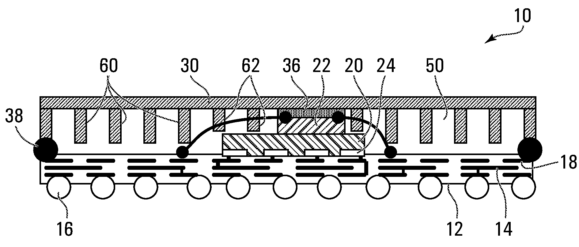
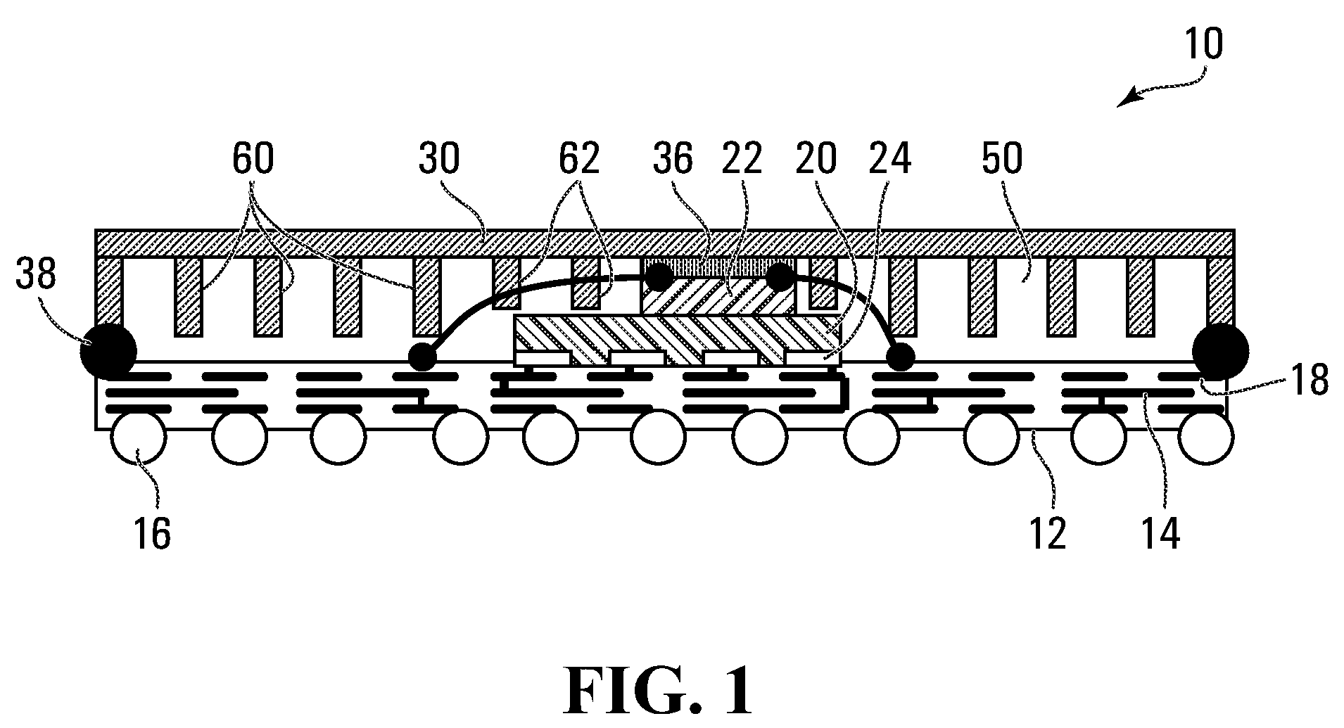
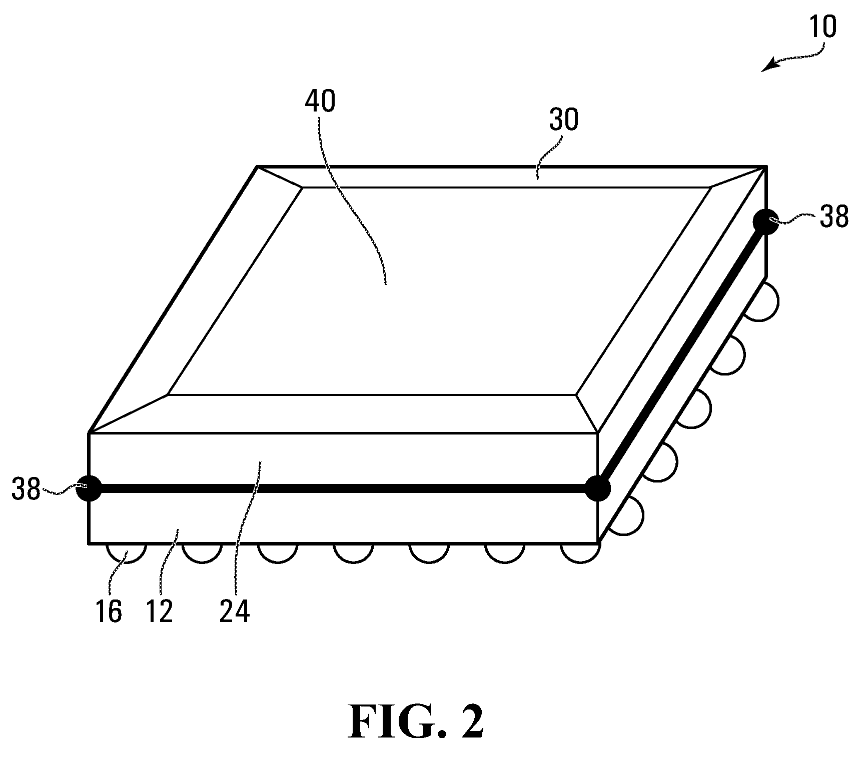
[0022]FIG. 1 shows a semiconductor device 10, exemplary of an embodiment of the present invention, in cross-section. As illustrated, semiconductor device 10 includes a substrate 12, several dies 20, 22, package pins 16 and a lid 30. As will become apparent, lid 30 acts as a heat spreader.

[0023]Formed within substrate 12 are multiple metallization layers 14 formed proximate the bottom surface of substrate 12. Metallization layers 14 may be connected to each other with microvias 18, and electrically interconnect dies 20, 22 to package pins 16.

[0024]Exemplary substrate 12 is single sided: metallization layers 14 are formed only proximate one side of substrate 12. Conveniently, in a single sided substrate, plated through holes which may span the entire height of the substrate between metallization layers on opposite sides of the substrate are avoided. Of course, substrate 12 could be replaced with a dual sided substrate.

[0025]Package pins 16, may be pins, solder balls arranged in ball g...


PUM


Abstract

A semiconductor device includes first and second stacked semiconductor dies on a substrate. A lid having a plurality of fins extending downwardly into the cavity is mounted on the substrate to encapsulate the semiconductor dies. At least some of the fins are longer than other ones of said fins. The lid is attached to the substrate, with the longer fins extending downwardly above a region of the substrate not occupied by the first die. The shorter fins extend downwardly above a region of said first die not covered by said second die. A thermal interface material fills the remainder of the cavity and is in thermal communication with both dies, the substrate and the fins. The lid may be molded from metal. The lid may be bonded to the topmost die, using a thermal bonding material that may be liquid metal, or the like.

Description

FIELD OF THE INVENTION[0001]The present invention relates generally to semiconductor devices and more particularly to semiconductor packages for stacked semiconductor dies.BACKGROUND OF THE INVENTION[0002]Current semiconductor devices typically include a die, a substrate, one or more metallization layers, I / O pins or balls, a heat spreader and optionally a heat sink. The die contains the active circuitry of the device. The die is typically mounted on the substrate or in a cavity within the substrate. One or more of the metallization layers include pads called bond-fingers that are used to interconnect the metallization layers to die-pads of the die. The die pads are, in turn, interconnected with the active circuitry of the die. The metallization layers route electrical connections within the substrate from the die to the I / O pins or balls.[0003]The die-pads may be electrically coupled to the bond-fingers using conventional wire bonding, by connecting the pads to the bond-fingers by ...

Claims


Application Information

Patent Timeline
Patent Type & Authority Applications(United States)
IPC IPC(8): H01L23/34H01L21/50
CPCH01L23/10H01L2225/06568H01L23/38H01L23/42H01L23/427H01L25/0657H01L2224/32145H01L2224/48091H01L2224/48145H01L2225/06506H01L2225/06589H01L2924/01079H01L2924/14H01L2924/15311H01L23/36H01L2225/06558H01L24/48H01L2225/06517H01L2924/00014H01L2224/45099H01L2224/45015H01L2924/207H01L2924/00012H01L23/31
Inventor REFAI-AHMED, GAMAL
Owner ATI TECH INC
Why Eureka
Try Eureka